OLED (Organic Light-Emitting Diode) display panel packaging structure and packaging method

A display panel and packaging structure technology, which is applied in the field of OLED display panels, can solve the problems of package failure, poor user experience, screen wiring and circuit damage, etc., to improve the packaging effect, realize narrow frame display, reduce Effect of border size

Active Publication Date: 2017-07-07
KUNSHAN GO VISIONOX OPTO ELECTRONICS CO LTD
View PDF6 Cites 21 Cited by
  • Summary
  • Abstract
  • Description
  • Claims
  • Application Information

AI Technical Summary

Problems solved by technology

Frit coating adopts screen printing, and the width generally reaches hundreds of microns. In addition, there are circuits and other traces on the edge of the display area, so the frame of the screen is still relatively wide (above 1mm), and the user experience is still not enough. it is good
At the same time, due to the need to use laser to melt Frit, the temperature is relatively high, which is easy to damage the wiring and circuits around the screen. The packaging effect of Frit is often affected by the air bubbles in the Frit paste, resulting in package failure.

Method used


Image

  • OLED (Organic Light-Emitting Diode) display panel packaging structure and packaging method
  • OLED (Organic Light-Emitting Diode) display panel packaging structure and packaging method
  • OLED (Organic Light-Emitting Diode) display panel packaging structure and packaging method

Examples


Embodiment Construction

[0027] In order to further explain the technical means and effects of the present invention to achieve the intended purpose of the invention, the specific implementation, structure, features and effects of the present invention will be described in detail below in conjunction with the accompanying drawings and examples.

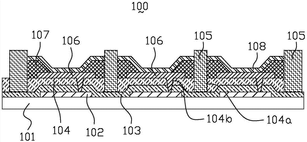
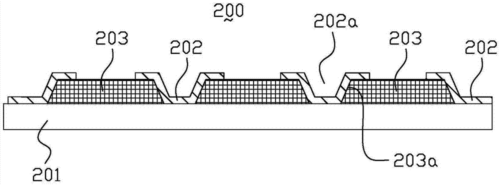
[0028] An embodiment of the present invention provides a packaging structure of an OLED display panel, which includes a substrate 100 and a cover 200, and is formed by two parts of the substrate 100 and the cover 200, respectively as follows figure 1 and figure 2 shown.

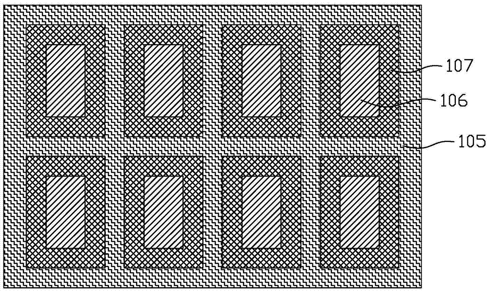
[0029] Please refer to figure 1 , the substrate 100 includes a first substrate 101, a plurality of pixel regions are formed on the first substrate 101, an OLED device 108 and a pixel circuit 102 for driving the OLED device 108 are formed in each pixel region, and the OLED device 108 is located in the pixel circuit 102 above. The substrate 100 forms a metal isolation wall 105 around the p...


PUM


Abstract

The invention discloses an OLED (Organic Light-Emitting Diode) display panel packaging structure and a packaging method. The packaging structure comprises a base plate and a cover plate, wherein the base plate comprises a first substrate; multiple pixel areas are formed on the first substrate; each pixel area is internally provided with an OLED device and a pixel circuit for driving the OLED device; the OLED device is located on the pixel circuit; the cover plate comprises a second substrate; a metal isolation wall is formed around the pixel area on the base plate; the metal isolation wall is vertical to the first substrate and protrudes against the surface of the OLED device; a metal layer is formed on the second substrate; the position of the metal layer is corresponding to that of the metal isolation wall; the melting point of the metal layer is lower than that of the metal isolation wall; and the metal layer and the metal isolation wall are welded to seal the OLED device inside the metal isolation wall. According to the embodiment of the invention, through forming the metal isolation wall around the pixel area, the welding metal layer is formed at the corresponding position on the cover plate, sealing between the cover plate and the base plate is realized through a hot pressing welding mode, the packaging effects are improved, and the screen body frame size can be reduced.

Description

technical field [0001] The present invention relates to the technical field of OLED display panels, in particular to a packaging structure and packaging method of OLED display panels. Background technique [0002] Organic light-emitting diode OLED (Organic Light-Emitting Diode) display, as a new type of flat panel display, has the characteristics of active light emission, high luminous brightness, high resolution, wide viewing angle, fast response speed, low energy consumption and flexibility. It has received more and more attention and has become a next-generation display technology that may replace liquid crystal displays. [0003] Organic layer materials that are extremely sensitive to water vapor and oxygen exist in the OLED display panel, which greatly reduces the lifespan of the OLED display panel. In order to solve this problem, in the prior art, various materials are mainly used to encapsulate the OLED display panel to protect the organic layer material. [0004] A...

Claims


Application Information

Patent Timeline
Patent Type & Authority Applications(China)
IPC IPC(8): H01L51/52H01L27/32
CPCH10K59/12H10K50/8423H10K50/8428H10K50/841
Inventor 周茂清段志勇魏朝刚
Owner KUNSHAN GO VISIONOX OPTO ELECTRONICS CO LTD
Why Eureka
Try Eureka