Wafer cleaning device and cleaning method thereof

A cleaning device and wafer technology, which are applied in cleaning methods and utensils, cleaning methods using tools, cleaning methods using liquids, etc., can solve the problem of scratches formed on the surface of wafers to be cleaned, cleaning brushes not being cleaned in time, The problem of low efficiency of cleaning brushes can avoid scratches, save production costs and prolong service life.

Inactive Publication Date: 2017-07-14
SEMICON MFG INT (SHANGHAI) CORP +1
View PDF9 Cites 15 Cited by
  • Summary
  • Abstract
  • Description
  • Claims
  • Application Information

AI Technical Summary

Problems solved by technology

[0006] In view of the above-mentioned shortcomings of the prior art, the object of the present invention is to provide a wafer cleaning device and its cleaning method, which is used to solve the problem that the cleaning brushes in the prior art cannot be cleaned in time, and it is easy to form on the surface of the wafer to be cleaned. Scratches, which in turn affect the quality of the wafer, and the low work efficiency caused by regular replacement of cleaning brushes, resulting in a waste of human and financial resources

Method used


Image

  • Wafer cleaning device and cleaning method thereof
  • Wafer cleaning device and cleaning method thereof
  • Wafer cleaning device and cleaning method thereof

Examples


Embodiment Construction

[0053] The implementation of the present invention will be illustrated by specific specific examples below, and those skilled in the art can easily understand other advantages and effects of the present invention from the contents disclosed in this specification.

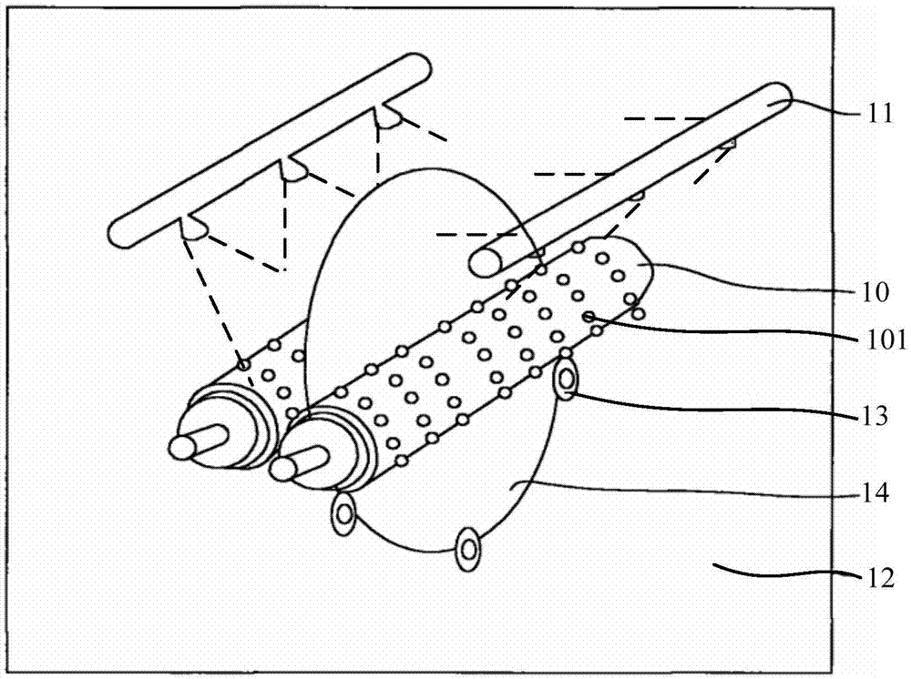
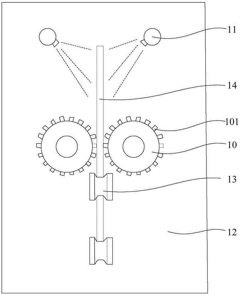
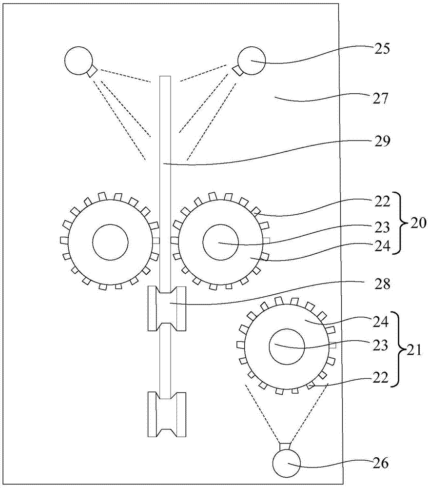
[0054] see Figure 3 to Figure 6. It should be noted that the structures, proportions, sizes, etc. shown in the drawings attached to this specification are only used to match the content disclosed in the specification, for those who are familiar with this technology to understand and read, and are not used to limit the implementation of the present invention. Limiting conditions, so there is no technical substantive meaning, any modification of structure, change of proportional relationship or adjustment of size, without affecting the effect and purpose of the present invention, should still fall within the scope of the present invention. The disclosed technical content must be within the scope covered. At the sam...


PUM


Abstract

The invention provides a wafer cleaning device and a cleaning method thereof. The wafer cleaning device at least comprises a first cleaning brush and a second cleaning brush. The first cleaning brush is used for scrubbing a wafer to be cleaned. The second cleaning brush is arranged parallel to the first cleaning brush and used for cleaning the first cleaning brush. By arranging the first cleaning brush and the second cleaning brush in the wafer cleaning device at the same time, after the wafer to be cleaned is scrubbed by the first cleaning brush, the second cleaning brush cleans the first cleaning brush, under the condition that the wafer scrubbing process is not affected, the first cleaning brush can be scrubbed, stains adhering to the surface of the first cleaning brush can be removed in time, and the situation that the wafer to be cleaned is scratched in the process of scrubbing the wafer to be cleaned is avoided. Thus, the scrubbing quality is guaranteed, the working efficiency is improved, the service life of the first cleaning brush is prolonged, and production cost is reduced.

Description

technical field [0001] The invention relates to the field of semiconductor preparation equipment, in particular to a wafer cleaning device and a cleaning method thereof. Background technique [0002] In the semiconductor manufacturing process, with the continuous upgrading of process technology, the requirements for the flatness of the wafer surface are getting higher and higher. The chemical mechanical polishing (CMP) technology is a combination of mechanical grinding and chemical corrosion. The chemical mechanical polishing technology uses the grinding effect of ultra-fine particles and the chemical corrosion of the slurry to form a smooth surface on the surface of the ground medium. The flat plane can realize the global planarization of the wafer surface. Chemical mechanical polishing technology is the product of the development of integrated circuits towards miniaturization, multilayering, thinning, and planarization. It has become the mainstream technology in the semic...

Claims


Application Information

Patent Timeline
Patent Type & Authority Applications(China)
IPC IPC(8): B08B1/02B08B3/02H01L21/02H01L21/67
CPCH01L21/02057H01L21/67023H01L21/67046H01L21/67051B08B3/022B08B1/12B08B1/20
Inventor 李松
Owner SEMICON MFG INT (SHANGHAI) CORP
Why Eureka
Try Eureka