

Display device structure and manufacturing method thereof
A technology for display devices and display modules, which is applied in the manufacture of semiconductor/solid-state devices, electric solid-state devices, semiconductor devices, etc., and can solve the problems of increasing the difficulty of bonding, reducing the bending characteristics of the panel, and uneven small bubbles on the bonding surface. problems, to avoid device damage and improve performance
- Summary
- Abstract
- Description
- Claims
- Application Information
AI Technical Summary
Problems solved by technology
Method used
Image

Examples
Embodiment 1
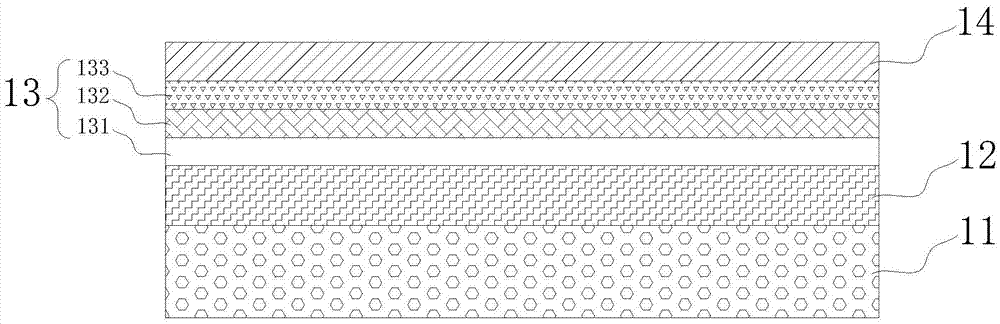
[0076] figure 1 It is a schematic diagram of the structure of a traditional flexible display device, figure 2 It is a schematic structural diagram of the display device in the embodiment of the present application; as figure 1 As shown, a display module 13 (including a display substrate 131, an organic light-emitting layer 132 and a thin film encapsulation layer 133) and a polarizer 14 are prepared on the upper surface of the flexible substrate 12 of a conventional display device, while the lower surface of the flexible substrate 12 is prepared There is a protective film 11; when this structure is used in the bonding process of device preparation, the active area of the panel (ie, the display module 13) is easily damaged due to the stress generated by the bonding process and other processes.
[0077] In order to effectively avoid damage to the active area of the panel caused by the stress generated by the bonding process and other processes, this application provides a n...
Embodiment 2
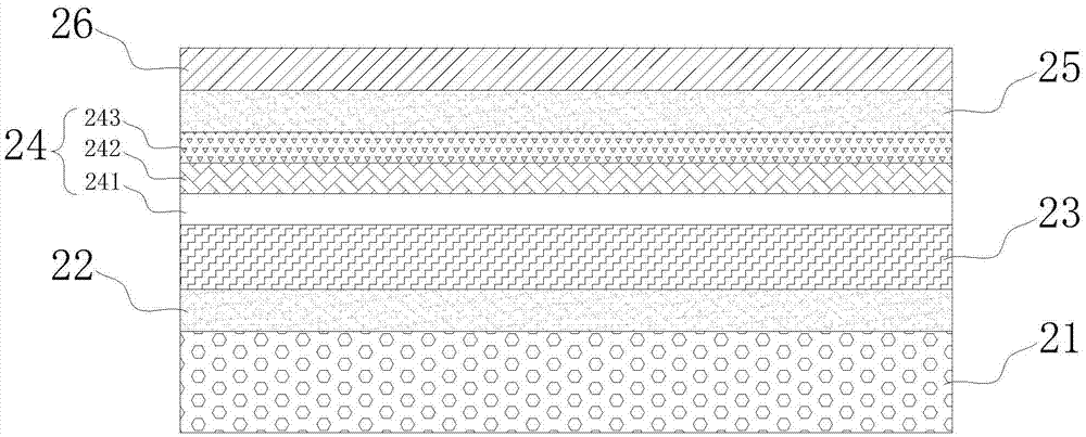
[0091] Based on the above-mentioned first embodiment, as Figure 2-4 This embodiment also provides a method for preparing a display device, which can be applied to the preparation of a flexible display device, and the method includes:
[0092] First, a flexible substrate 23 is provided having a front surface and a back surface opposite to the front surface.
[0093] Next, a display substrate 241 , an organic light-emitting layer 242 and a thin film encapsulation layer 243 are sequentially prepared on the front surface of the flexible substrate 23 to form the display module 24 of the display device.
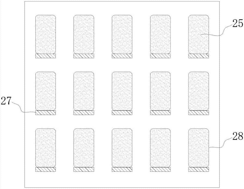
[0094] Afterwards, continue the inkjet printing process, if the ink viscosity is less than 20cps and the surface tension is 20-35mN / m 2 , the spraying material is acrylate (acrylate) or silicone resin (silicone), etc., on the upper surface of the display module 24 (ie, the upper surface of the film encapsulation layer 243) and the back surface of the flexible substrate 23. The th...
PUM
| Property | Measurement | Unit |
|---|---|---|
| Thickness | aaaaa | aaaaa |
| Viscosity | aaaaa | aaaaa |
Abstract
Description
Claims
Application Information