Porous film getter structure and preparation method thereof

A porous film and porous structure technology, applied in the field of high vacuum MEMS device packaging, can solve the problems of weak three-dimensional structure, weak adhesion of film getters and sidewalls, contamination of devices, etc., to maintain vacuum and use Extended life, increased suction performance and service life, uniform distribution effect

Pending Publication Date: 2021-12-10
安徽光智科技有限公司
View PDF0 Cites 0 Cited by
  • Summary
  • Abstract
  • Description
  • Claims
  • Application Information

AI Technical Summary

Problems solved by technology

At present, there are related patents to increase the deposition area of ​​the getter by preparing a vertical three-dimensional structure of bumps and grooves inside the cavity. First, the simple concave-convex structure designed by this patent has a limited increase in the deposition area of ​​the getter.
In addition, the three-dimensional structure of bumps and grooves is weak, and the most critical thing is that the thin film getter deposited on the smooth side wall has weak adhesion to the side wall, and the weak adhesion of the film to the side wall is very easy to make During the use of the device, the thin film getter falls off, contaminates the inside of the device, and causes the performance of the thermal unit of the device to decline or even fail. Moreover, the three-dimensional getter structure prepared by the related

Method used


Image

  • Porous film getter structure and preparation method thereof
  • Porous film getter structure and preparation method thereof
  • Porous film getter structure and preparation method thereof

Examples


Embodiment 1

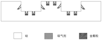
[0054] A porous thin film getter structure such as figure 1 As shown, including the wafer and the film getter, the upper surface of the wafer has a plurality of groove structures, the inner walls of the groove structures are all porous structures, and the wafer surface connecting adjacent groove structures is also A porous structure, the porous structure is provided with a thin film getter, and the thin film getter covers the porous structure.

[0055] Gold particles are arranged on the pore bottom of the porous structure, and the thin film getter covers the gold particles. The particle diameter of the gold particles is between tens of nanometers and several micrometers, which can be adjusted according to the required structural size of the thin film getter.

[0056] The cross section of the groove structure is " "shape.

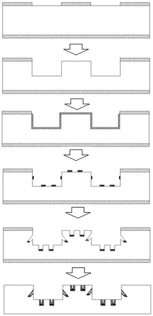
[0057] The above-mentioned porous thin film getter structure, that is, the production of the capped silicon wafer, the specific preparation process diag...

Embodiment 2

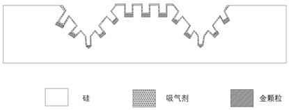
[0072] A porous thin film getter structure such as image 3 As shown, it includes a wafer and a film getter, the upper surface of the wafer has a groove structure, the inner wall of the groove structure is a porous structure, the porous structure is provided with a film getter, and the A thin film getter covers the porous structure.

[0073] Gold particles are arranged on the pore bottom of the porous structure, and the thin film getter covers the gold particles. The particle size of the gold particles is tens of nanometers to several micrometers; the cross section of the groove structure is V-shaped.

[0074] The wafer is provided with more than two groove structures, and the surface of the wafer connecting adjacent groove structures is a porous structure, and a thin film getter is provided on the porous structure, and the thin film getter covers the the porous structure.

[0075] The above-mentioned porous thin film getter structure, that is, the production of the capped ...


PUM

PropertyMeasurementUnit
Sizeaaaaaaaaaa
Thicknessaaaaaaaaaa
Thicknessaaaaaaaaaa

Abstract

The invention discloses a porous film getter structure. Theporous film getter structure comprises a wafer and a film getter, the upper surface of the wafer is provided with a groove structure, the inner wall of the groove structure is of a porous structure, and the porous structure is covered with the film getter. The invention further discloses a preparation method of the structure, dry or wet etching is combined with gold particle auxiliary etching to form the three-dimensional film getter structure, and the porous structure is prepared on the prepared groove structure to increase the deposition area and deposition volume of the film getter, so that the getter performance of the film getter is effectively improved, and the service life of the film getter is effectively prolonged. The gold film deposited through the evaporation-stripping process can form uniformly distributed gold particles on the side wall and the substrate of the groove under the process condition of high-temperature rapid annealing, the annealed gold particles are used for carrying out the etching process, uniformly distributed porous structures are etched on the side wall, the adhesion of the getter film, the side wall and the bottom substrate is further improved, and the phenomena of falling of the getter, device damage and the like are avoided.

Description

technical field [0001] The invention belongs to the field of high-vacuum MEMS device packaging, and specifically relates to a porous film getter structure and a preparation method thereof. Background technique [0002] At present, the requirements for the internal vacuum degree and service life of devices in the field of high-vacuum MEMS packaging are getting higher and higher, especially the electronic devices are getting closer to miniaturization, so how to maintain a high vacuum degree and Service life has become a technical difficulty. In today's electronic packaging field, the most common vacuum maintenance method is to evaporate a thin film getter inside the electronic device. The characteristic of the thin film getter is to continuously absorb the residual gas, infiltrating gas and residual adsorbed gas inside the cavity. . So as to meet the requirement of maintaining the vacuum degree inside the electronic device. [0003] The getter performance of thin film gette...

Claims


Application Information

Patent Timeline
IPC IPC(8): B81B7/00B81B7/02B81C1/00
CPCB81B7/0038B81B7/02B81C1/00285
Inventor 赵龙杨晓杰李海涛姚浩强高玉波赵雪城
Owner 安徽光智科技有限公司
Why Eureka
Try Eureka