Semiconductor wafer composed of monocrystalline silicon and method for producing itö

a monocrystalline silicon and monocrystalline silicon technology, applied in the field of monocrystalline silicon monocrystalline silicon and the method of producing ito, can solve the problems of no longer being detected by a cop test, the average diameter of these agglomerates is so small, and the thickness of not more than 7 nm to undergo breakdown, etc., to achieve good gettering properties, high yield, and free of defects

Active Publication Date: 2010-03-11
SILTRONIC AG
View PDF14 Cites 12 Cited by
  • Summary
  • Abstract
  • Description
  • Claims
  • Application Information

AI Technical Summary

Benefits of technology

[0014]Therefore, an object of the present invention was to provide a semiconductor wafer composed of monocrystalline silicon which has good gettering properties and is substantially free of defects, in particular with regard to OSFs and OSF nuclei, in a region relevant to the integration of electronic devices. Furthermore, the object of the present invention was to specify a very economical method which can supply such semiconductor wafers in a high yield. These and other objects are achieved by growing a single crystal by the CZ method under conditions of V and G such that the crystal contains both a Pv region and an OSF region and doping with oxygen and nitrogen are controlled during the growth process, wafers are sawn from the single crystal, and subjected to a specific heat treatment at elevated temperature. The wafers have a high and uniform BMD distribution, and an OSF region extending radially outward from the center of the wafer, with a low OSF density.

Problems solved by technology

Furthermore, even OSF nuclei can cause thin gate oxides having a thickness of not more than 7 nm to undergo breakdown.
The size of the BMDs used as getters must not fall below a critical size because small BMDs are not thermally stable and are eliminated in the course of thermal treatments of the semiconductor wafer that are performed during the production of electronic components.
If the point defects attain supersaturation during the cooling of the single crystal, they form agglomerates which, in the case of the vacancies, are the cause of the production of COPs.
However, the average diameter of these agglomerates is so small that they are no longer detected by a COP test.
No account is taken of the fact that measures for avoiding harmful OSF nuclei have to be taken as soon as the OSF region is included, and that difficulties as a result of COP formation are virtually unavoidable as soon as a vacancy-rich region is present inside an OSF ring.
However, many difficulties have to be overcome in this regard.
In the case of semiconductor wafers which originate from the end portion of the single crystal processed to form semiconductor wafers, the comparatively high concentration of nitrogen can have the effect that they have an excessively high number of OSF nuclei since nitrogen promotes the oxygen precipitation necessary for the nucleation.
However, the number of OSF nuclei is not only dependent on the concentration of nitrogen, since semiconductor wafers which originate from the front part of the single crystal section processed to form semiconductor wafers can also have an excessively high number of OSF nuclei.

Method used


Image

  • Semiconductor wafer composed of monocrystalline silicon and method for producing itö
  • Semiconductor wafer composed of monocrystalline silicon and method for producing itö
  • Semiconductor wafer composed of monocrystalline silicon and method for producing itö

Examples


Embodiment Construction

)

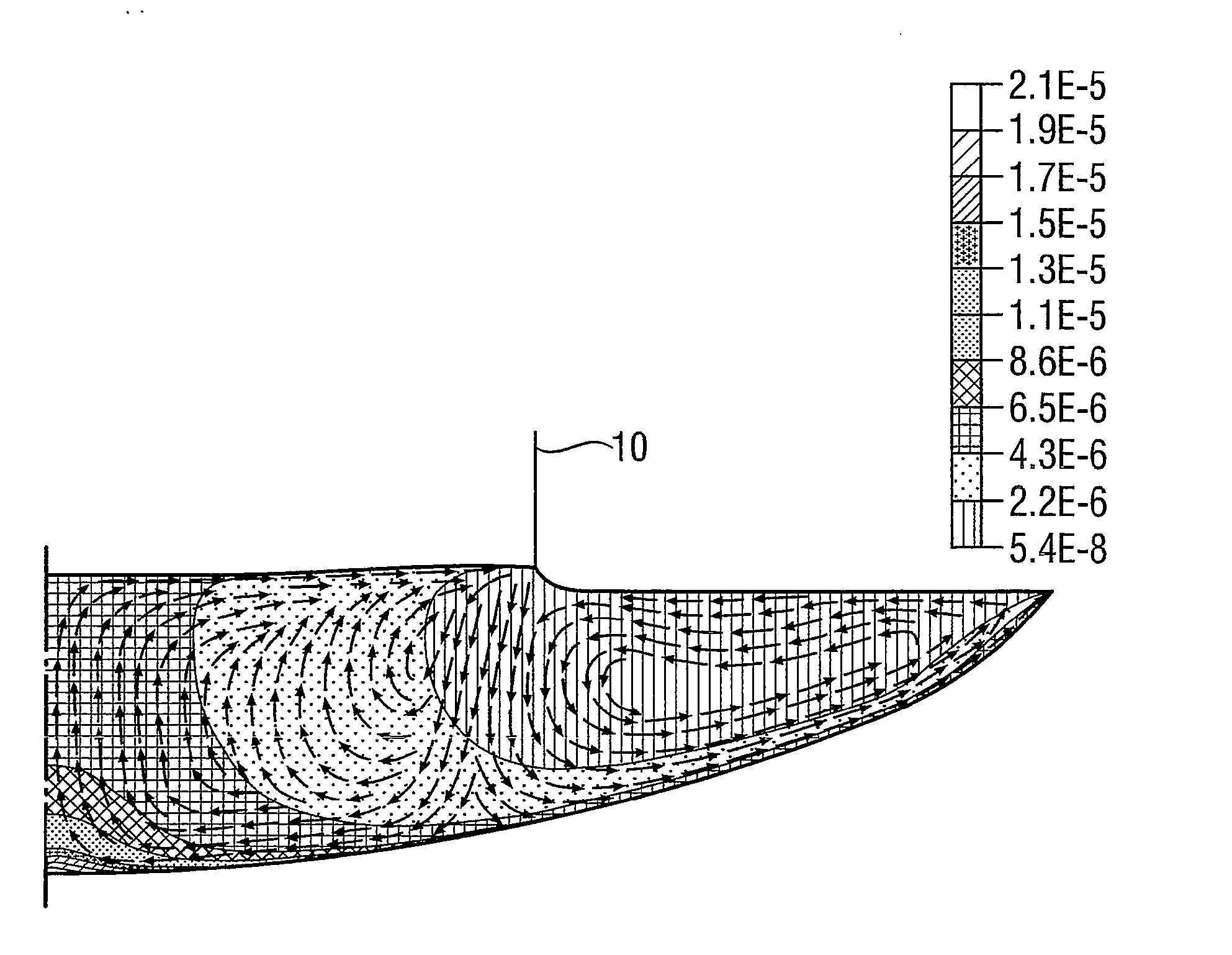
[0028]The invention is thus directed to a semiconductor wafer composed of monocrystalline silicon, the wafer being doped with nitrogen, and furthermore comprising: an OSF region and a Pv region, wherein the OSF region extends from the center of the semiconductor wafer in the direction toward the edge of the semiconductor wafer as far as the Pv region; a BMD density in the bulk of at least 3.5×108 cm−3; a radial distribution of the BMD density with a fluctuation range expressed by the quotient BMDmax / BMDmin of not more than 3, where BMDmax and BMDmin represent the maximum and minimum BMD density, respectively; and an OSF density of less than 10 cm−2.

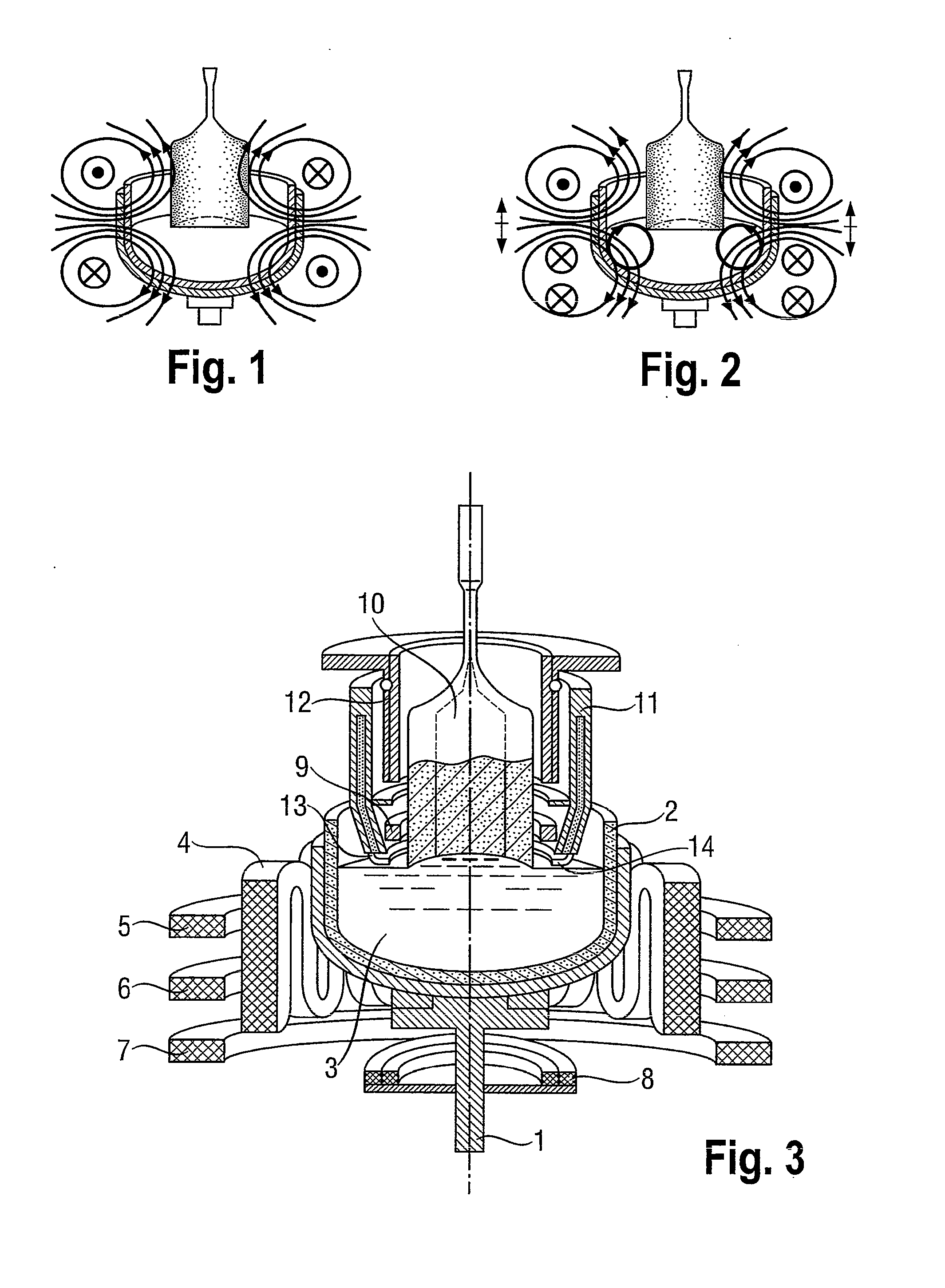
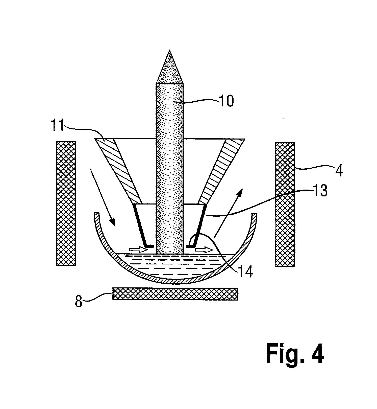
[0029]The invention is furthermore directed to a method for producing semiconductor wafers composed of monocrystalline silicon, comprising: pulling a single crystal from a melt in accordance with the CZ method, and during the process of pulling the single crystal, controlling the quotient V / G of the pulling rate V and the axial temperatu...


PUM


Abstract

Semiconductor wafers composed of monocrystalline silicon and doped with nitrogen contain an OSF region and a PV region, wherein the OSF region extends from the center radially toward the edge of the wafer as far as the Pv region; the wafer has an OSF density of less than 10 cm−2, a BMD density in the bulk of at least 3.5×108 cm−3, and a radial distribution of the BMD density with a fluctuation range BMDmax/BMDmim of not more than 3. The wafers are produced by controlling initial nitrogen content and maintaining oxygen within a narrow window, followed by a heat treatment.

Description

CROSS-REFERENCE TO RELATED APPLICATIONS[0001]This application claims priority to German application DE 10 2008 046617.4 filed Sep. 10, 2008, which is herein incorporated by reference.BACKGROUND OF THE INVENTION[0002]1. Field of the Invention[0003]The invention relates to a semiconductor wafer composed of monocrystalline silicon which has good gettering properties and is substantially free from defects in a region relevant to the integration of electronic devices. The invention also relates to an economical method for producing such semiconductor wafers.[0004]2. Background Art[0005]Two central requirements are made of a high-performance semiconductor wafer composed of monocrystalline silicon with regard to the defect distribution. Thus, the region of the semiconductor wafer into which the electronic devices are integrated must be as free as possible from defect types having a size in the range of the size of the structure widths of the electronic components or larger. These defect ty...

Claims


Application Information

Patent Timeline
Patent Type & Authority Applications(United States)
IPC IPC(8): H01L29/30H01L21/18
CPCC30B15/04C30B15/203C30B33/02C30B29/06C30B30/04C30B15/305C30B15/00
Inventor MUELLER, TIMOKISSINGER, GUDRUNHEUWIESER, WALTERWEBER, MARTIN
Owner SILTRONIC AG
Why Eureka
Try Eureka