Method for Producing Soi Wafer

a technology of silicon on insulator and soi, which is applied in the direction of semiconductor/solid-state device manufacturing, basic electric elements, electric apparatus, etc., can solve the problems of increased harmful effect of metal contamination, increased impurities, and disadvantages of soi wafer structure, and achieves high degree of uniformity in film thickness

Active Publication Date: 2009-04-23
SHIN-ETSU HANDOTAI CO LTD
View PDF11 Cites 15 Cited by
  • Summary
  • Abstract
  • Description
  • Claims
  • Application Information

AI Technical Summary

Benefits of technology

[0009]Thus the present invention has been completed in view of such problems and an object of the present invention is to provide a method for efficiently producing an SOI wafer having a polycrystalline silicon layer uniform in thickness introduced in the neighborhood of a buried insulator layer and having high gettering ability for metal impurities in the SOI layer by a convenient and cost-effective method.
[0011]In a method for producing an SOI wafer having such steps, when the step of ion-implanting argon, at least before the bonding step, from the surface of either the base wafer or the bond wafer at the dosage of 1×10¹⁵ atoms / cm2 or more is included, the surface ion-implanted with argon is used as a bonding surface in the bonding step, and the increase rate of temperature to the treatment temperature of the bonding heat treatment is 5° C. / minute or higher, a polycrystalline silicon layer having a flat surface and a high degree of uniformity in film thickness is formed immediately under or directly on a buried insulator layer and an SOI wafer added with excellent gettering ability is efficiently produced in simple steps at a low cost. Moreover, because a film thickness of a polycrystalline silicon layer is controlled by the acceleration voltage of ion-implanting, the controllability of the film thickness of the polycrystalline silicon layer is high.
[0017]When the insulator film is a silicon oxide film, a silicon nitride film, or a combination of these as mentioned above, a fine, high-quality insulator film is easily formed and an SOI wafer excellent in both an insulating property and gettering ability can be produced.
[0022]According to the present invention, there can efficiently be produced an SOI wafer in which a polycrystalline silicon layer having a flat interface and a high degree of uniformity in film thickness is formed in simple steps. An SOI wafer having such a polycrystalline silicon layer formed thereon is also more effective for the gettering of metal impurities in the SOI layer.

Problems solved by technology

Although the SOI wafer has a lot of structural advantages in view of electrical characteristics as described above, the SOI wafer has structural disadvantages in view of resistance to contamination with metal impurities.
Thereby, in the case of a contamination from an SOI layer surface, the metal impurities accumulate in the thin SOI layer due to the difficulty for the metal impurities to pass the Box layer.
Thus a harmful effect of metal contamination is increased as compared with a silicon substrate having no SOI structures.
However, even if a gettering layer is introduced on the support substrate according to the similar techniques, the above-mentioned gettering layer does not function fully due to the difficulty for the metal impurities to pass the Box layer, thus there is a problem in that these techniques are not to be applied to an SOI wafer as they are.
However, in a method in which a polycrystalline silicon layer is introduced in the neighborhood of the Box layer by a CVD method mentioned above, due to the inconstancy of a film thickness of the polycrystalline silicon layer produced by a CVD method, a complicated process, as is represented by mirror polishing required before bonding, has been required.
Such being the case, there has been a problem in that the cost is increased and productivity is lowered.
There has also been a problem in that variation in crystalline interface influences the mirror polishing process to widen variation of a thickness of the polycrystalline silicon layer, leading to variation in a thickness of the SOI layer.

Method used


Image

  • Method for Producing Soi Wafer
  • Method for Producing Soi Wafer
  • Method for Producing Soi Wafer

Examples


examples

[0072]Hereinafter, the present invention is described more specifically showing examples of the present invention, but these examples should by no means be construed as limiting the present invention.

examples 1 and 2

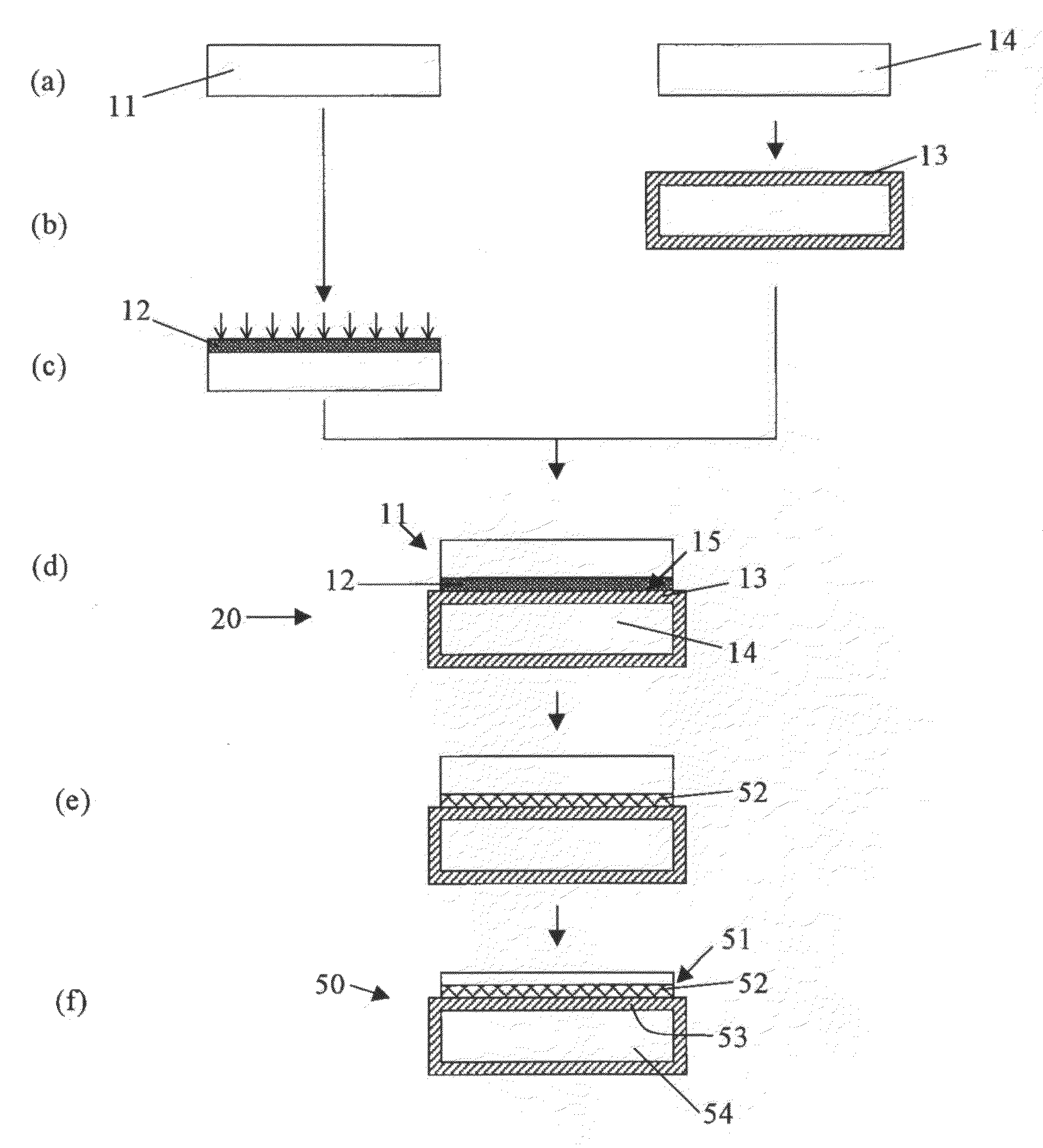
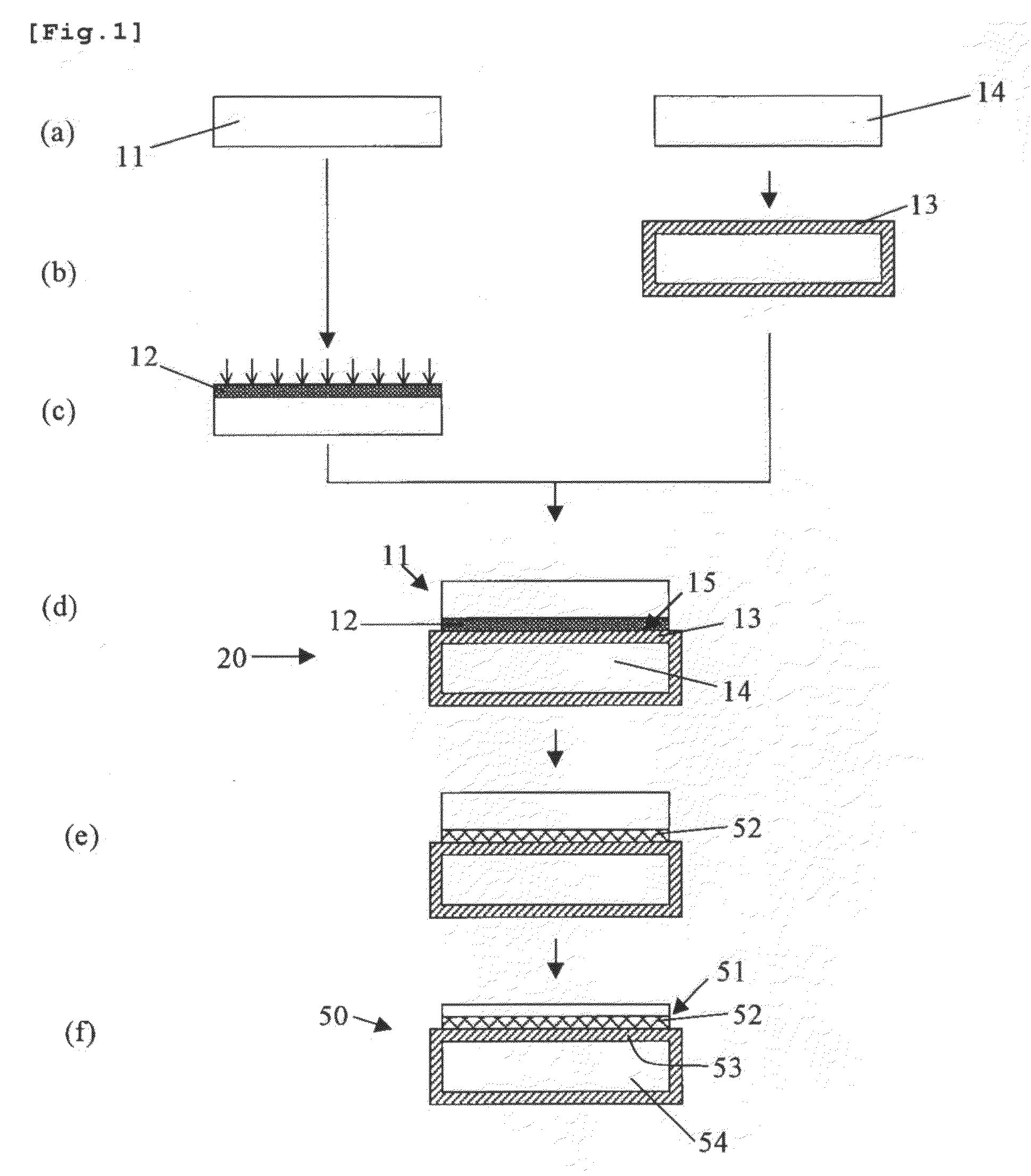
[0073]According to the steps as shown in FIG. 1, there were produced SOI wafers in which a polycrystalline silicon layer had been introduced as described in the following.

[0074]First there were prepared two mirror-polished N-type silicon single crystal wafers 725 μm in thickness, 200 mm in diameter, a plane orientation of {100} (a). On a surface of the base wafer 14, there was formed a silicon oxide film 13 approximately 1 μm in thickness to serve as a Box layer by thermal oxidation (b).

[0075]Then, onto the surface of the bond wafer 11, argon was ion-implanted at an acceleration voltage of keV and at a dosage of 1×10¹⁵ atoms / cm2 (Example 1) or 4×10¹⁶ atoms / cm2 (Example 2).

[0076]Next, the bond wafer 11 and the base wafer 14 were, with a surface of the bond wafer 11 ion-implanted with argon as a bonding surface, brought into contact and bonded together in such a way that a silicon oxide film 13 was put in between (d). Subsequently, a bonding heat treatment for increasing the bond stre...

example 3

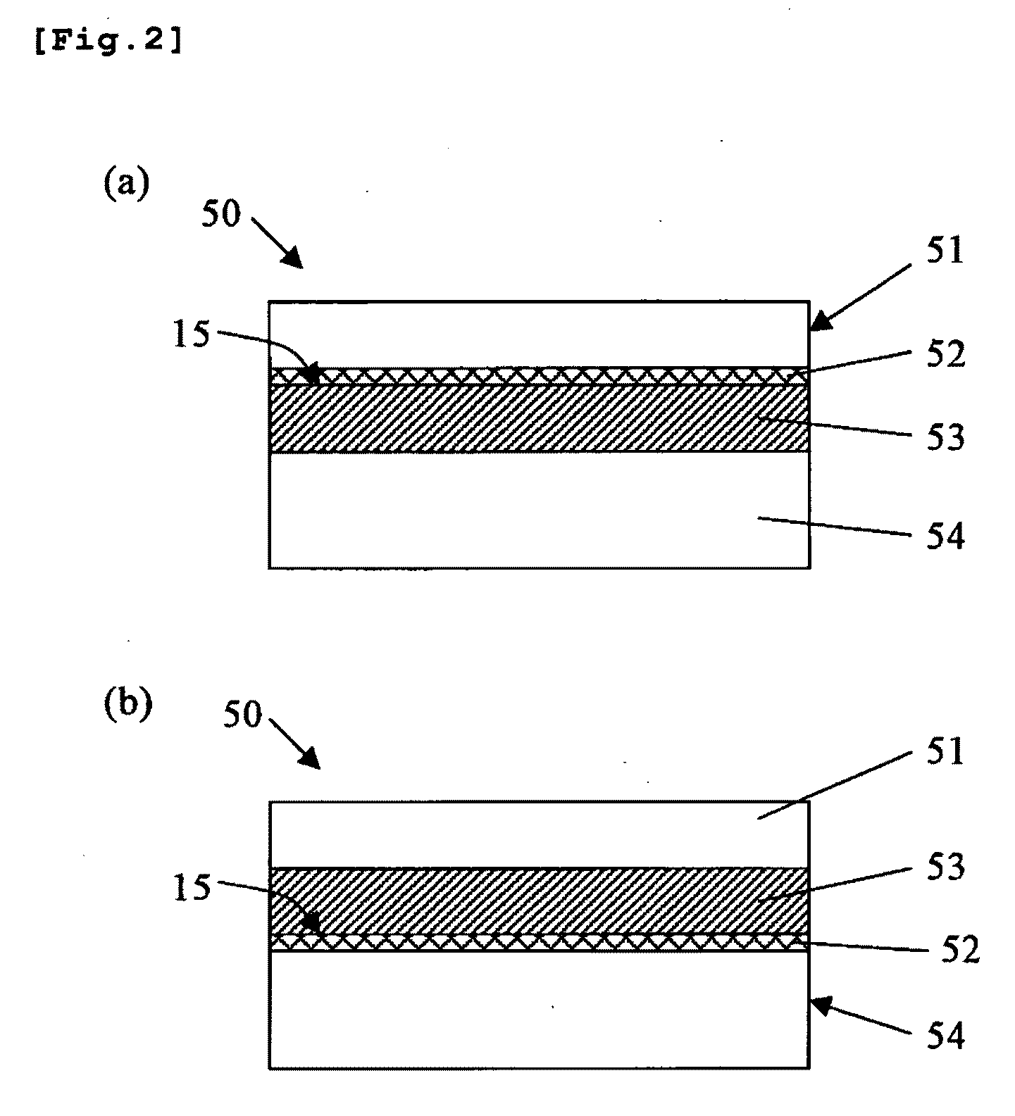
[0084]An SOI wafer having a structure as shown in FIG. 2 (b) was produced in a method similar to the one used in Example 1 except that the base wafer 14 is ion-implanted with argon at a dosage of 4×10¹⁶ atoms / cm2 and that an oxide film approximately 50 nm in thickness was formed on the bond wafer 11. Then according to the technique similar to the one in Example 1, gettering ability was evaluated and the result is shown in FIG. 7.

[0085]As a result, it was found that Ni was trapped in the 2 μm-thick surface of the base wafer and that the SOI wafers of Example 3, with this surface as a gettering layer, had high gettering ability.


PUM

PropertyMeasurementUnit
temperatureaaaaaaaaaa
thicknessaaaaaaaaaa
thicknessaaaaaaaaaa

Abstract

The present invention relates to a method for producing an SOI wafer, having at least a step of a bonding heat treatment for increasing bonding strength by heat-treating a bonded wafer obtained by bonding a base wafer and a bond wafer, in which argon is ion-implanted from a surface of either the base wafer or the bond wafer at a dosage of 1×10¹⁵ atoms / cm2 or more at least before the bonding step, the surface ion-implanted with argon is used as a bonding surface in the bonding step, and an increase rate of temperature to a treatment temperature of the bonding heat treatment is 5° C. / minute or higher. Thus the present invention provides a method for producing an SOI wafer facilitating the efficient production of an SOI wafer having in the neighborhood of a buried insulator layer thereof a polycrystalline silicon layer uniform in thickness introduced and having high gettering ability toward metal contaminations in the SOI layer by a simple and low-cost method.

Description

TECHNICAL FIELD[0001]The present invention relates to a method for producing an SOI (Silicon on Insulator) wafer by a bonding method and particularly to a method for producing an SOI wafer added with gettering ability by introducing a polycrystalline silicon layer in the neighborhood of a buried insulator layer.BACKGROUND ART[0002]SOI wafers have recently been used to produce highly integrated CMOSs, ICs, high breakdown voltage devices and the like. A concrete structure of an SOI wafer is comprised of a three-layer structure in the depth direction of the wafer as follows: a silicon single crystal layer (hereinafter referred to as an SOI layer) that is a surface layer and is used as an active layer providing an area for fabricating a device; a buried insulator layer (hereinafter sometimes referred to as a Box layer in the case of a silicon oxide film) such as an oxide film put under the silicon single crystal layer; and another silicon single crystal layer (hereinafter referred to as...

Claims


Application Information

Patent Timeline
Patent Type & Authority Applications(United States)
IPC IPC(8): H01L21/762
CPCH01L21/76256H01L21/26506H01L21/20
Inventor YOSHIDA, KAZUHIKOMATSUMINE, MASAOTAKENO, HIROSHI
Owner SHIN-ETSU HANDOTAI CO LTD
Why Eureka
Try Eureka