FPGA (Field-Programmable Gate Array) device upgrading method and system based on Ethernet link

A technology of Ethernet and equipment, applied in the computer field, can solve the problem of inconvenient opening of the equipment shell

Inactive Publication Date: 2017-08-01
COMMANDING AUTOMATION TECHN RANDD & APPL CENT THE FOURTH ACADEMY CASIC
View PDF2 Cites 7 Cited by
  • Summary
  • Abstract
  • Description
  • Claims
  • Application Information

AI Technical Summary

Problems solved by technology

[0004] The technical problem to be solved by the present invention is to provide a method for upgrading FPGA equipment based on an Ethernet link, which solves the inconvenience of using a dedicated upgrading device to upgrade equipment using FPGA in the prior art and needs to open the equipment shell. question

Method used


Image

  • FPGA (Field-Programmable Gate Array) device upgrading method and system based on Ethernet link
  • FPGA (Field-Programmable Gate Array) device upgrading method and system based on Ethernet link
  • FPGA (Field-Programmable Gate Array) device upgrading method and system based on Ethernet link

Examples


Embodiment 1

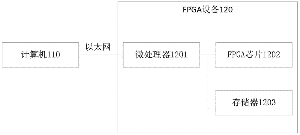
[0030] The embodiment of the present invention discloses an FPGA device upgrade system based on Ethernet link, such as figure 1 Said, the system includes: FPGA device 120 to be upgraded and computer 110, wherein:

[0031] The FPGA device 120 to be upgraded is provided with a microprocessor 1201, a memory 1203, and an FPGA chip 1202;

[0032] The computer 110 and the FPGA device are connected through an Ethernet interface, and a data frame for establishing a link is sent to the FPGA device 120 through the Ethernet interface, so that the FPGA device 120 establishes an upgrade link with the computer;

[0033] The microprocessor 1201 is connected to the memory 1203 through an SPI bus, and is configured to write the binary program file read from the computer into the memory 1203;

[0034] The FPGA chip 1202 is connected to the memory 1203 via an SPI bus, and is used to read the binary program file stored in the memory 1203 connected to it.

[0035] The upgrade system disclosed in the embodim...

Embodiment 2

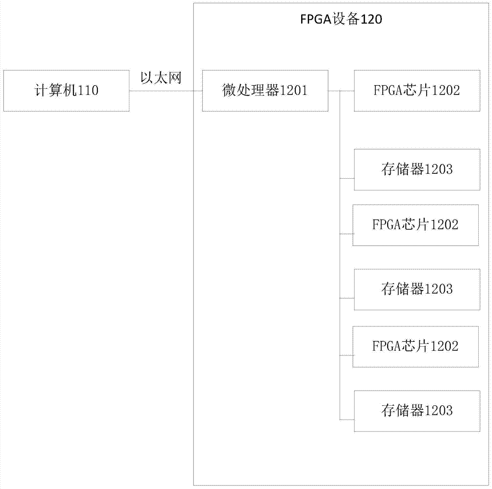
[0037] In another specific embodiment of the present invention, such as figure 2 As shown, the FPGA device 120 to be upgraded is provided with multiple FPGA chips 1202, and each of the FPGA chips 1202 is respectively connected to the microprocessor 110 through an SPI bus.

[0038] Correspondingly, during specific implementation, the FPGA device 120 to be upgraded is provided with the same number of memories 1203 as the FPGA chips 1202, and each piece of the FPGA chip 1202 is connected to a piece of memory 1203 via an SPI bus. Each piece of memory 1203 is used to store the upgrade code file of the FPGA chip 1202 connected to it.

[0039] By configuring a piece of memory for each FPGA chip, parallel upgrades can be realized and the efficiency of FPGA device upgrades can be improved.

Embodiment 3

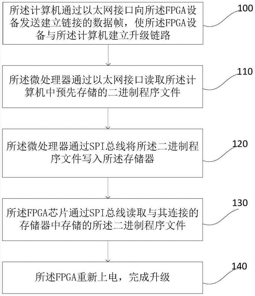
[0041] Correspondingly, the embodiment of the present invention also discloses a method for upgrading an FPGA device based on an Ethernet link, which is applied to the FPGA device upgrade system based on an Ethernet link disclosed in the first and second embodiments. Such as image 3 As shown, the upgrade method includes:

[0042] Step 100: The computer sends a data frame for establishing a link to the FPGA device through an Ethernet interface, so that the FPGA device and the computer establish an upgrade link;

[0043] Step 110: The microprocessor reads the binary program file pre-stored in the computer through the Ethernet interface;

[0044] Step 120: The microprocessor writes the binary program file into the memory via the SPI bus;

[0045] Step 130: The FPGA chip reads the binary program file stored in the memory connected to the FPGA chip through the SPI bus;

[0046] Step 140: The FPGA is powered on again to complete the upgrade.

[0047] The upgrade method disclosed in the embod...


PUM


Abstract

The invention provides a FPGA (Field-Programmable Gate Array) device upgrading system based on an Ethernet link, which belongs to the technical field of computers. The upgrading system comprises a to-be-upgraded FPGA device and a computer, wherein a microprocessor reads a binary program file pre-stored in the computer through an Ethernet interface; the microprocessor writes the binary program file to a memory through an SPI bus; an FPGA chip reads the binary program file stored in the connected memory through the SPI bus; and the FPGA is power-on again to complete upgrading. In comparison with the prior art, when the FPGA device is upgraded, remote upgrading can be realized without opening the shell of the FPGA device, and the upgrading is more convenient.

Description

Technical field [0001] The invention relates to the field of computer technology, in particular to a method and system for upgrading an FPGA device based on an Ethernet link. Background technique [0002] FPGA (Field-Programmable Gate Array), the field programmable gate array, is a product of further development on the basis of programmable logic devices. It emerged as a semi-custom circuit in the field of application-specific integrated circuits (ASIC), which not only solves the shortcomings of custom circuits, but also overcomes the shortcomings of the limited number of gate circuits of the original programmable devices. The circuit design completed with hardware description language (Verilog or VHDL) can be quickly burned to FPGA for testing after simple synthesis and layout, which is the mainstream of modern IC design verification technology. The FPGA circuit can be quickly finished, and can be modified to correct errors in the program to upgrade the program. Therefore, with...

Claims


Application Information

Patent Timeline
Patent Type & Authority Applications(China)
IPC IPC(8): H04L12/24
CPCH04L41/082
Inventor 刘庆侯树艳崔丹
Owner COMMANDING AUTOMATION TECHN RANDD & APPL CENT THE FOURTH ACADEMY CASIC
Why Eureka
Try Eureka