
Solar Cell And Method Of Manufacturing The Same

A solar cell and electrode technology, applied in the direction of final product manufacturing, sustainable manufacturing/processing, circuits, etc., can solve problems such as low efficiency and low productivity

Active Publication Date: 2017-08-11
SHANGRAO JINKO SOLAR TECH DEV CO LTD
View PDF8 Cites 3 Cited by
  • Summary
  • Abstract
  • Description
  • Claims
  • Application Information

AI Technical Summary

Problems solved by technology

In order to commercialize solar cells, it is necessary to overcome the problems of low efficiency and low productivity, and thus solar cells and their manufacturing methods that can maximize the efficiency and productivity of solar cells are required

Method used


Image

  • Solar Cell And Method Of Manufacturing The Same
  • Solar Cell And Method Of Manufacturing The Same
  • Solar Cell And Method Of Manufacturing The Same

Examples


manufacture example 1

[0158] A protective film layer formed of a silicon oxide film is formed on one surface of the n-type single crystal semiconductor substrate. A first semiconductor portion containing polysilicon and having a first crystal grain size is formed on the protective film layer via low pressure chemical vapor deposition. It is formed by irradiating the intrinsic semiconductor layer with laser light to grow crystal grains in the portion of the intrinsic semiconductor layer separated from the protective film layer while retaining the first semiconductor portion in the portion of the semiconductor layer close to the protective film layer The second semiconductor layer. At this time, the first crystal grain size is 50 nm, the second crystal grain size is 250 nm, the difference between the first crystal grain size and the second crystal grain size is 200 nm, and the ratio of the second crystal grain size to the first crystal grain size is 5:1. In addition, one region of the first semicond...

manufacture example 2

[0167] The solar cell was manufactured via the same method as the first solar cell of Manufacturing Example 1, except that the thickness of the second portion was 10% with respect to the thickness of the entire conductive region.

manufacture example 4

[0171] The solar cell was manufactured via the same method as the first solar cell of Manufacturing Example 1, except that the thickness of the second portion was 88% with respect to the thickness of the entire conductive region.

[0172] in Figure 13 Illustrated in the first solar cell according to Manufacturing Example 1, the first comparative solar cell according to Manufacturing Example 1, and the solar cells according to Comparative Example 2 and Manufacturing Examples 2 to 4 of the carrier mobility in the first conductive region relative value.

[0173] Reference Figure 13 It can be seen that the carrier mobility in the first solar cell according to Manufacturing Example 1 is higher than that in the first comparative solar cell according to Comparative Example 1. On the other hand, it can be seen that when the solar cell according to Comparative Example 2 has a carrier mobility similar to that of the solar cell according to Comparative Example 1, and therefore has a crystal...


PUM


Abstract

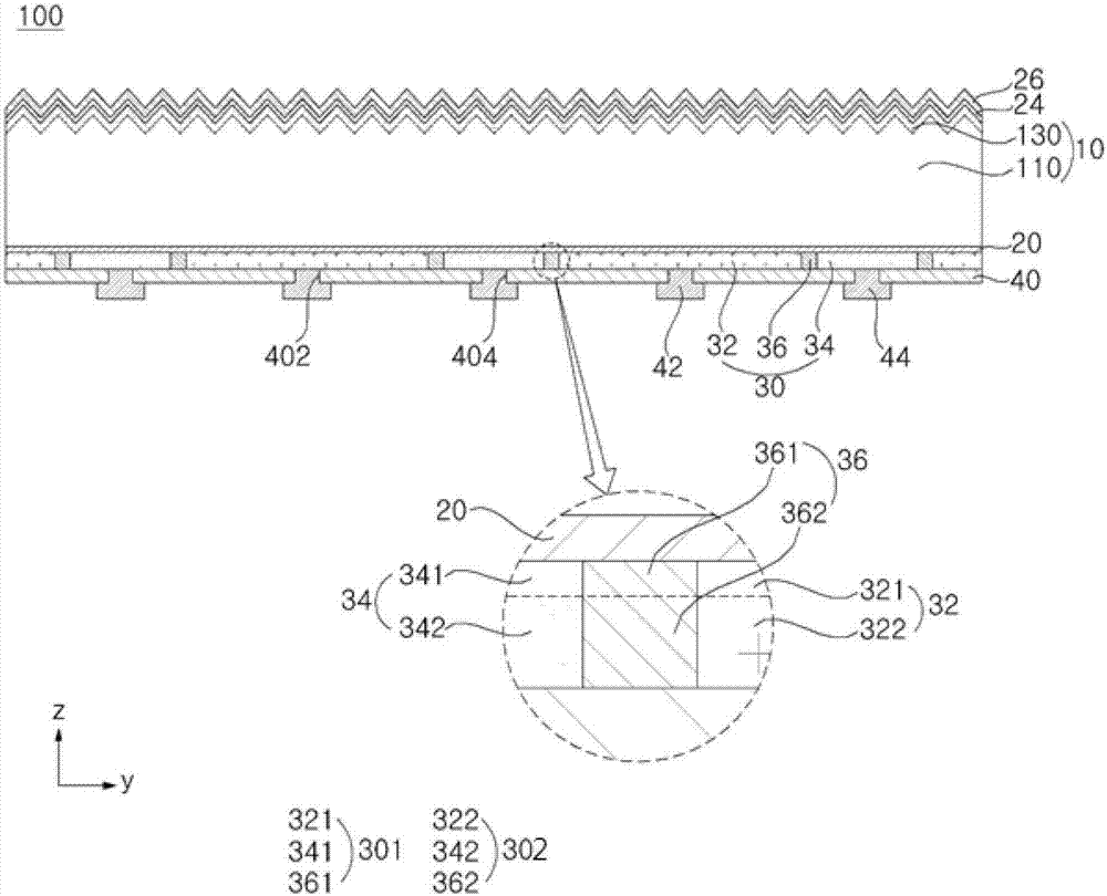
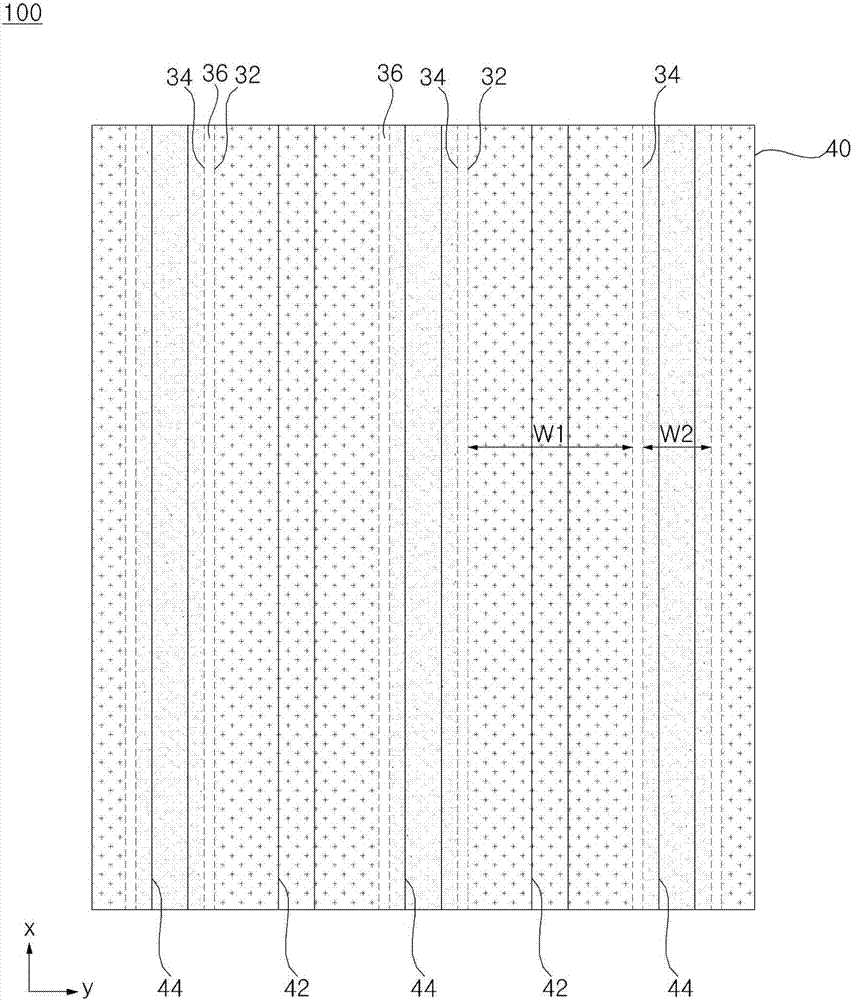
Disclosed is a solar cell including a semiconductor substrate, a protective-film layer formed over one surface of the semiconductor substrate, a first conductive area disposed over the protective-film layer, the first conductive area being of a first conductive type and including a crystalline semiconductor, and a first electrode electrically connected to the first conductive area. The first conductive area includes a first portion disposed over the protective-film layer and having a first crystal grain size, and a second portion disposed over the first portion and having a second crystal grain size, which is greater than the first crystal grain size.

Description

Technical field [0001] The invention relates to a solar cell with an improved structure and a manufacturing method thereof. Background technique [0002] Recently, due to the consumption of existing energy sources such as oil and coal, the number of alternative energy sources used to replace the existing energy sources is increasing. Most importantly, solar cells are popular next-generation batteries used to convert sunlight into electrical energy. [0003] The solar cell can be manufactured by forming various layers and electrodes based on a specific design. The efficiency of the solar cell can be determined by the design of various layers and electrodes. In order to commercialize solar cells, it is necessary to overcome the problems of low efficiency and low productivity, and therefore there is a need for solar cells and manufacturing methods thereof that can maximize the efficiency and productivity of solar cells. Summary of the invention [0004] According to one aspect of th...

Claims


Application Information

Patent Timeline
Patent Type & Authority Applications(China)
IPC IPC(8): H01L31/02H01L31/068H01L31/18
CPCH01L31/02008H01L31/068H01L31/1804H01L31/022441H01L31/0368Y02E10/547H01L31/02167H01L31/0682H01L31/1872Y02P70/50H01L31/036
Inventor 李有真郑镇元池光善
Owner SHANGRAO JINKO SOLAR TECH DEV CO LTD
Features
  • Generate Ideas
  • Intellectual Property
  • Life Sciences
  • Materials
  • Tech Scout
  • Unparalleled Data Quality
  • Higher Quality Content
  • 60% Fewer Hallucinations
Learn More