Light emitting device having asymmetric light shape and manufacturing method thereof

A technology for a light-emitting device and a manufacturing method, which is applied in the directions of electrical components, circuits, semiconductor devices, etc., can solve the problems of increasing the size and space of the CSP light-emitting device, increasing the production cost, and lack of it.

Active Publication Date: 2017-08-11
MAVEN OPTRONICS CO LTD
View PDF14 Cites 10 Cited by
  • Summary
  • Abstract
  • Description
  • Claims
  • Application Information

AI Technical Summary

Problems solved by technology

[0009] In terms of luminous characteristics, existing CSP LEDs can be divided into two types: top emitting and 5-surface emitting. Front emitting CSP LEDs use reflective materials to cover the four sides of the LED chip, and the light is only It is transmitted outward from the upper surface, so it has a small luminous angle (about 120°), and the light of the five-sided CSP LED can be transmitted outward from the upper surface and four sides, so it has a larger luminous angle (about 140°~ 160°), however, like bracket LEDs, these two types of CSP LEDs are both symmetrical light shapes, and cannot meet the application of asymmetric light shapes
In addition, for CSP LEDs, if a primary optical lens or a secondary optical lens is used to generate an asymmetric light shape, it will not only significantly increase the production cost, but also greatly increase the size of the CSP light-emitting device or its use. The space, so will lose the advantage of small size of CSPLED
However, the existing CSPLED still lacks an effective solution to achieve an asymmetric light shape.

Method used


Image

  • Light emitting device having asymmetric light shape and manufacturing method thereof
  • Light emitting device having asymmetric light shape and manufacturing method thereof
  • Light emitting device having asymmetric light shape and manufacturing method thereof

Examples


Embodiment Construction

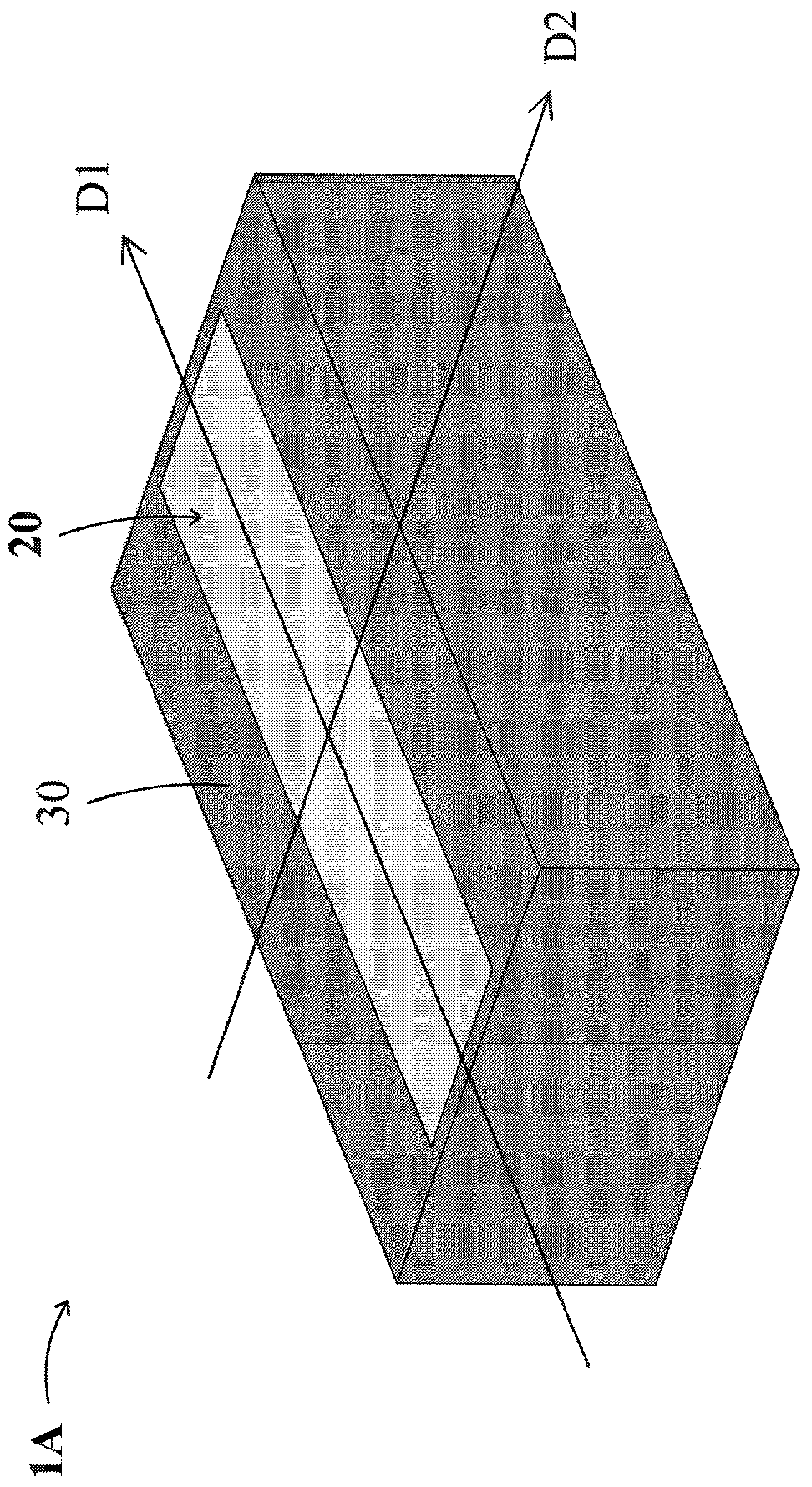
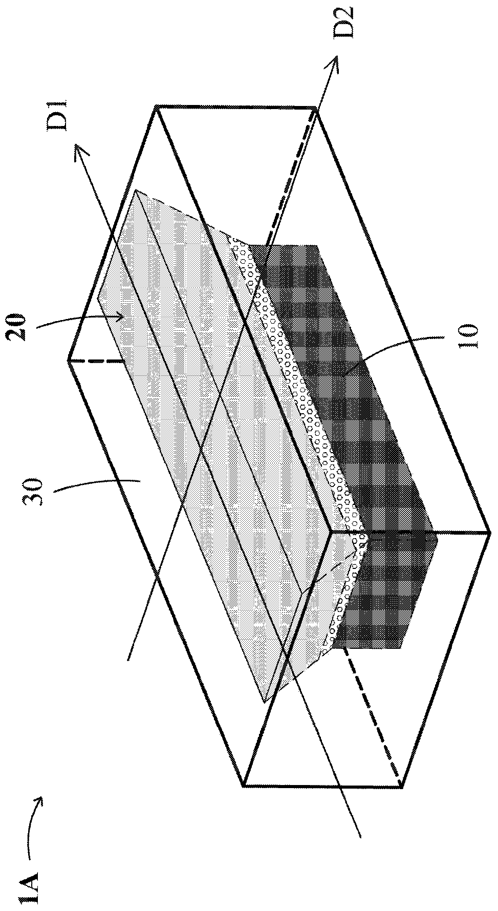
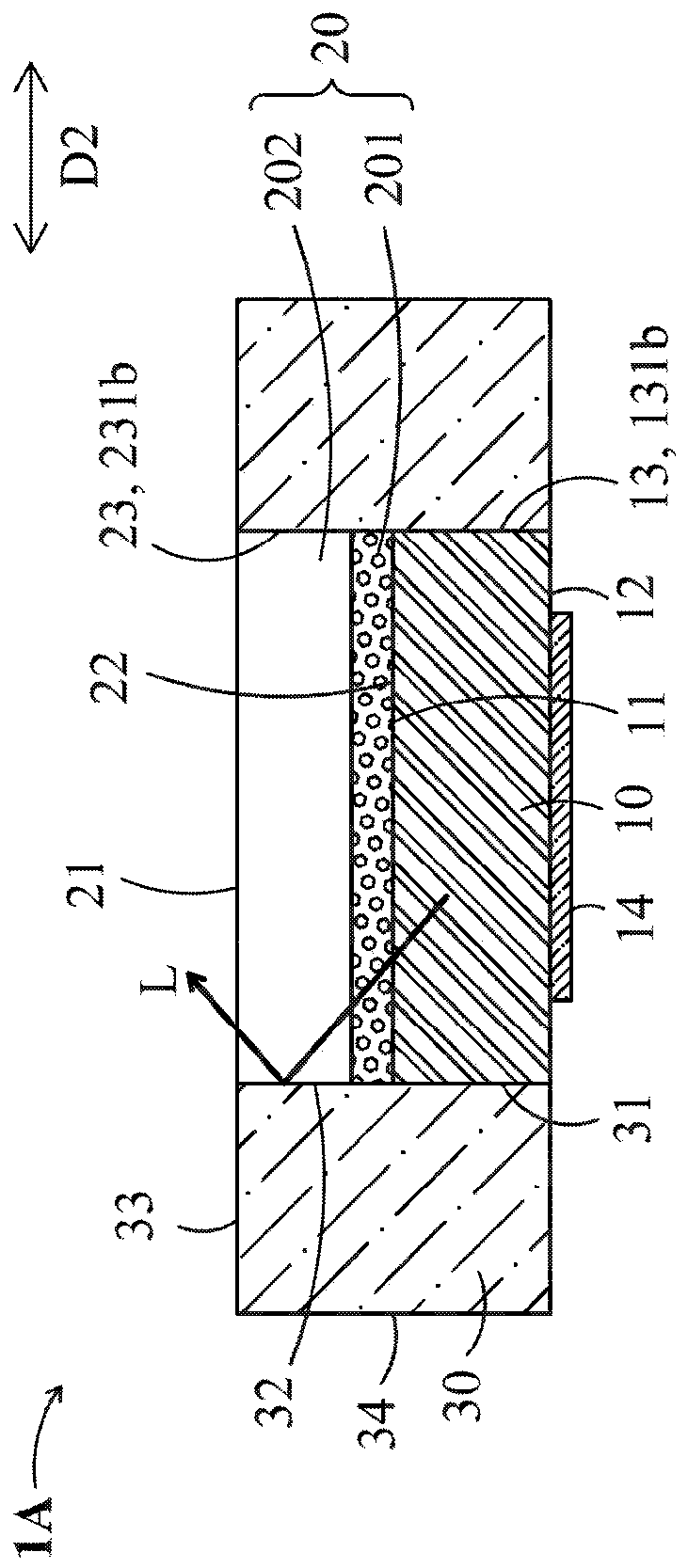
[0066] see Figure 1A to Figure 1D As shown, it is two perspective schematic diagrams and two cross-sectional schematic diagrams of the light emitting device according to the first preferred embodiment of the present invention. When the light emitting device 1A is used, it will occupy a certain area (not shown in the figure), and the area extends in a first horizontal direction D1 and a second horizontal direction D2, and the first horizontal direction D1 and the second horizontal direction D2 are mutually vertical, and each of the first horizontal direction D1 and the second horizontal direction D2 is perpendicular to the thickness direction (not shown) of the light emitting device 1A. The light emitting device 1A may include an LED chip 10 , a fluorescent structure 20 and a reflective structure 30 ; the technical content of these multiple components will be described in sequence as follows.

[0067] The LED chip 10 can be a flip-chip LED chip, and can have an upper surface ...


PUM


Abstract

The invention provides a monochromatic light chip scale packaging light emitting device having asymmetric light shape. The device comprises a flip-chip LED chip and a reflecting structure and can also comprise a florescent structure so as to form a white light chip scale packaging light emitting device having the asymmetric light shape. The florescent structure comprises a florescent layer and a light transmitting layer, and the bottom surface at least covers the upper surface of the LED chip. The reflecting structure at least partially shields the vertical surface of the LED chip and the side surface of the florescent structure. The invention also provides a manufacturing method of the light emitting device. Therefore, the light emitting angle of the chip scale packaging light emitting device can be effectively limited in a specific direction so as to provide the asymmetric light shape, and thus the application requirements of asymmetric lighting or light source can be met without using additional optical lens and the application advantage of small size can also be maintained.

Description

[0001] 【Technical field】 [0002] The present invention relates to a light emitting device and a manufacturing method thereof, in particular to a chip scale packaging (CSP) light emitting device including a flip-chip LED chip and a manufacturing method thereof. [0003] 【Background technique】 [0004] LED (light emitting device) chips are commonly used to provide lighting sources or configured in electronic products as backlights or indicator lights, and LED chips are usually placed in a package structure and covered with a fluorescent material or reflective material Wrap or cover to become a light emitting device. [0005] Among them, the widely used bracket type (PLCC-type) LED can be divided into two categories according to the light emitting direction: top-view type and side-view type. Front-facing LEDs are widely used as light sources for general lighting or backlights for direct-lit LCD TVs, while side-facing LEDs are widely used as backlights for edge-lit LCD TVs and mo...

Claims


Application Information

Patent Timeline
Patent Type & Authority Applications(China)
IPC IPC(8): H01L33/50H01L33/60
CPCH01L33/505H01L33/60H01L2933/0041
Inventor 陈杰王琮玺
Owner MAVEN OPTRONICS CO LTD
Why Eureka
Try Eureka