Check patentability & draft patents in minutes with Patsnap Eureka AI!

Photodetector, image sensor, and image sensor manufacturing method

An image sensor and photodiode technology, applied in the field of image sensors, can solve the problems of damage and need of underlying electronic devices

Inactive Publication Date: 2017-08-18
OMNIVISION TECH INC
View PDF4 Cites 0 Cited by
  • Summary
  • Abstract
  • Description
  • Claims
  • Application Information

AI Technical Summary

Problems solved by technology

However, the additional processing steps used to fabricate these structures can result in damage to the underlying electronics or require many additional process steps

Method used


Image

  • Photodetector, image sensor, and image sensor manufacturing method
  • Photodetector, image sensor, and image sensor manufacturing method
  • Photodetector, image sensor, and image sensor manufacturing method

Examples


Embodiment Construction

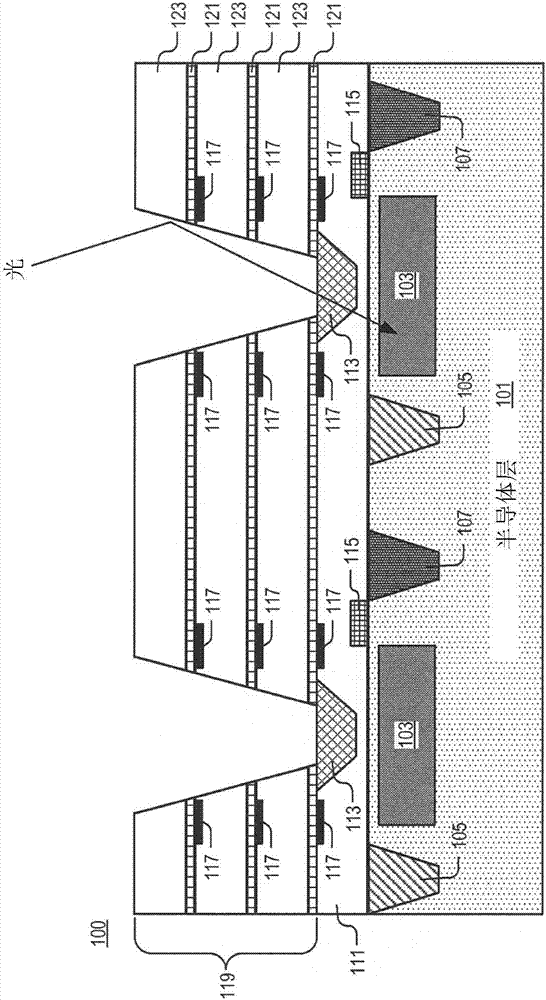
[0013] Examples of apparatus and methods for image sensors with optical channels are described herein. In the following description, several specific details are set forth in order to provide a thorough understanding of the embodiments. One skilled in the art will recognize, however, that the techniques described herein may be practiced without one or more of the specific details or with other methods, components, materials, etc. In other instances, well-known structures, materials, or operations have not been shown or described in detail to avoid obscuring certain aspects.

[0014] Reference throughout this specification to "one example" or "one embodiment" means that a particular feature, structure, or characteristic described in connection with the example is included in at least one example of the present invention. Thus, the appearances of the phrase "in one instance" or "in one embodiment" in various places in this specification are not necessarily all referring to the ...


PUM


Abstract

The present application relates to a photodetector, an image sensor, and an image sensor manufacturing method. The image sensor includes a plurality of photodiodes disposed in a semiconductor layer, a first isolation layer, and a dielectric filler. The dielectric filler is disposed in a trench in the first isolation layer, and the first isolation layer is disposed between the semiconductor layer and the dielectric filler. At least one additional isolation layer is disposed proximate to the first isolation layer, and a plurality of light channels in the at least one additional isolation layer extend through the at least one additional isolation layer to the dielectric filler. The plurality of light channels is disposed to direct light into the plurality of photodiodes.

Description

technical field [0001] The present invention relates generally to image sensors, and in particular, but not exclusively, to the construction of optical channels in image sensors. Background technique [0002] Image sensors have become ubiquitous. Image sensors are widely used in digital still cameras, cellular phones, and surveillance cameras, as well as in media, automotive, and other applications. The technology used to manufacture image sensors continues to advance at a rapid rate. For example, demands for higher resolution and lower power consumption encourage further miniaturization and integration of these devices. [0003] Image sensor performance is directly related to the number of photons that reach (and are absorbed by) a photodiode included in the image sensor. Typically, photodiodes are buried under many layers of the device architecture. An extra layer between the light source and the photodiode can cause photons incident on the image sensor to scatter and ...

Claims


Application Information

Patent Timeline
Patent Type & Authority Applications(China)
IPC IPC(8): H01L27/146
CPCH01L27/14627H01L27/1463H01L27/14643H01L27/14683H01L27/14685H01L27/14625H01L27/14636
Inventor 钱胤戴森·H·戴缪佳君陆震伟
Owner OMNIVISION TECH INC
Features
  • R&D
  • Intellectual Property
  • Life Sciences
  • Materials
  • Tech Scout
  • Unparalleled Data Quality
  • Higher Quality Content
  • 60% Fewer Hallucinations
Learn More