Supercharge Your Innovation With Domain-Expert AI Agents!

Electroluminescence device and its preparation method and application

An electroluminescent device and electrode technology, which is applied in the direction of electric solid-state devices, semiconductor/solid-state device manufacturing, electrical components, etc., can solve the problems of thin film uniformity and other problems, so as to improve uniformity and life, improve resolution, and improve The effect of longevity

Active Publication Date: 2019-08-09
GUANGDONG JUHUA PRINTING DISPLAY TECH CO LTD
View PDF5 Cites 0 Cited by
  • Summary
  • Abstract
  • Description
  • Claims
  • Application Information

AI Technical Summary

Problems solved by technology

The sensitivity of ink drying and film formation, as well as the complexity of many factors, make the existing drying and film formation process very vulnerable to any slight disturbance or defect of any factor, resulting in film failure even if each factor is well controlled. problem with uniformity

Method used


Image

  • Electroluminescence device and its preparation method and application
  • Electroluminescence device and its preparation method and application

Examples


Embodiment 1

[0033] Embodiment 1 (imprint template is plane):

[0034] In this embodiment, a method for preparing a printed electroluminescent device, the steps include:

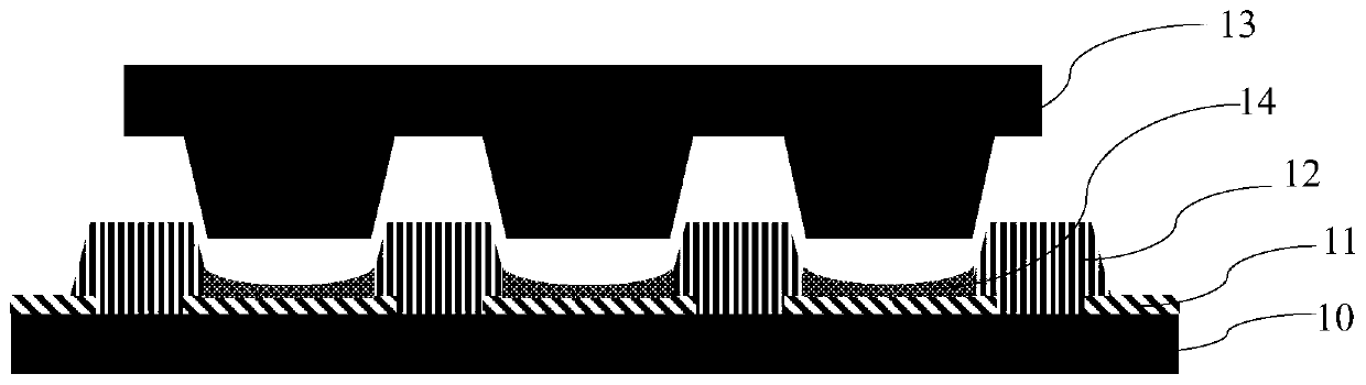
[0035] (1) The embossing template is prepared on a plane structure, and one or more identical embossing templates can be installed on the production line to planarize the functional layer material films of different layers and avoid cross-contamination;

[0036] (2) Obtain the base substrate, prepare an anode layer on the base substrate according to a conventional method, and coat a layer of bank film material (specifically polyimide high-density film) on the anode layer (pixel electrode) with a coating process. Molecule), embossing the embossing template on the bank film material, so that the bank film material forms a plurality of concave parts matching the convex parts, each of the concave parts corresponds to a pixel, and adopts photolithography technology to remove the bank film material at the bottom of the recess...

Embodiment 2

[0043] Embodiment 2 (the embossing template is a curved surface):

[0044] In this embodiment, a method for preparing a printed electroluminescent device, the steps include:

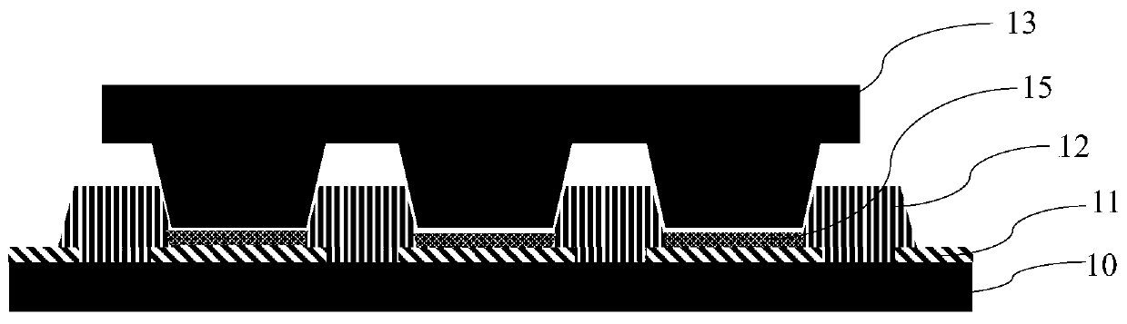
[0045] (1) Fix or directly process the embossing template on one or more rollers of roll-to-roll (hereinafter abbreviated as R2R) equipment. The size is set, and one or more identical embossing template rollers can be installed on the production line to planarize the functional layer material films of different layers and avoid cross-contamination;

[0046] (2) Obtain the base substrate (flexible substrate), and make an anode layer (pixel electrode) on the base substrate (flexible substrate) according to the conventional method; coat a layer of bank film material on the anode layer with R2R coating process (specifically polyimide polymer material), embossing the embossing template on the bank film material, so that the bank film material forms a plurality of concave parts matching the convex parts, each...


PUM


Abstract

The invention relates to an electroluminescent device and its preparation method and application. The preparation method comprises the following steps: obtaining a base substrate; obtaining an embossing template on which a plurality of protrusions are arranged; coating the base substrate A layer of bank film material is embossed on the bank film material using an embossing template, so that the bank film material forms a plurality of concave parts matching the convex parts, and then removes the bank film material at the bottom of the concave parts to form pixels Define the layer; fill the concave part with the functional layer material by inkjet printing or coating process, dry it in vacuum, then use the imprint template to carry out imprinting operation, and obtain the functional layer after baking and drying; repeat the above steps to prepare multiple functional layers layer; prepare the other electrode in a pair of electrodes, that is, an electroluminescent device. The method of the invention can effectively solve the film uniformity problem faced in the manufacturing process of the printed electroluminescent device, obtain a smooth film, and improve the service life of the electroluminescent device.

Description

technical field [0001] The invention relates to the field of display technology, in particular to an electroluminescent device display device and its preparation method and application. Background technique [0002] In the current manufacturing process of the printed electroluminescent device display panel, a layer of material for defining pixels must be used, and the pixel defining layer is usually called a bank. The currently widely used process is to use the inkjet printing process to fill the ink into each pixel area, and the ink is spread in the area surrounded by the bank; then, vacuum drying is carried out at a certain temperature (such as low temperature). By strictly controlling the solvent The volatilization rate, solvent vapor pressure and other parameters are used to ensure uniform drying in different areas within the pixel and among different pixels; finally, the film is completely dried by baking. However, using existing methods, equipment and process conditio...

Claims


Application Information

Patent Timeline
Patent Type & Authority Patents(China)
IPC IPC(8): H01L51/00H01L51/56H01L27/32H01L21/77
CPCH10K59/122H10K71/12H10K71/135H10K71/821H10K59/1201H10K71/00
Inventor 李哲
Owner GUANGDONG JUHUA PRINTING DISPLAY TECH CO LTD
Features
  • R&D
  • Intellectual Property
  • Life Sciences
  • Materials
  • Tech Scout
  • Unparalleled Data Quality
  • Higher Quality Content
  • 60% Fewer Hallucinations
Learn More