Antenna module and circuit module

一种天线模块、电介质的技术,应用在电路、天线、天线阵列等方向,能够解决多层模块固定力变弱等问题,达到提高散热特性的效果

Active Publication Date: 2017-08-18
MURATA MFG CO LTD
View PDF9 Cites 22 Cited by
  • Summary
  • Abstract
  • Description
  • Claims
  • Application Information

AI Technical Summary

Problems solved by technology

Therefore, the fixing force of the multilayer module becomes weaker

Method used


Image

  • Antenna module and circuit module
  • Antenna module and circuit module
  • Antenna module and circuit module

Examples


Embodiment 1

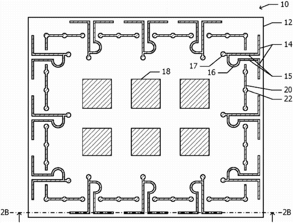
[0052] Reference Figure 1A ~ Figure 4 , The antenna module according to Embodiment 1 will be described.

[0053] Figure 1A This shows a horizontal cross-sectional view of the uppermost conductor layer in the dielectric substrate 12 used in the antenna module 10. The dielectric substrate 12 has a rectangular or square planar shape. The uppermost conductor layer includes multiple printed dipole antennas 14, power supply lines 15, baluns (baluns) 16, and multiple patch antennas 18. For the dielectric substrate 12, ceramics, epoxy resin, etc. are used, for example. The dipole antenna 14, the power supply line 15, the balun 16, and the patch antenna 18 use conductive materials such as copper, for example. Similarly, conductive materials such as copper are also used for the lower conductor layer.

[0054] The plurality of dipole antennas 14 are arranged along the outer circumference of the dielectric substrate 12 slightly inside of the outer circumference. Each of the dipole antenna...

Embodiment 2

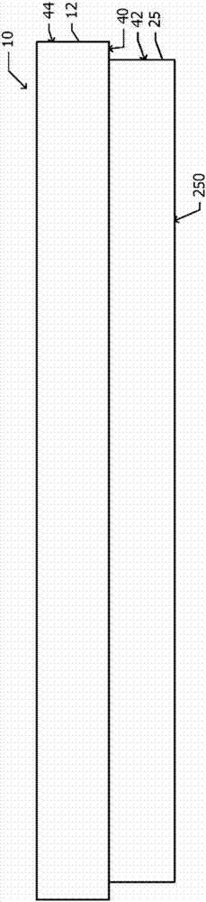
[0083] Reference Figure 6A as well as Figure 6B , The antenna module 10 according to the second embodiment will be described. Below, the comparison with Figure 1 to Figure 4 The illustrated difference of the antenna module 10 according to Embodiment 1 will be described, and the description of the common structure will be omitted. In Example 1, solder 36 ( Figure 4 ) Mount the antenna module 10 on the mounting substrate 60. In Embodiment 2, the NCP (non-conductive paste) method is adopted.

[0084] Figure 6A This shows a cross-sectional view of the antenna module 10 and the mounting board 60 before mounting. For example, a gold bump 37 is formed at the tip of the conductor post 30. The mounting area of ​​the antenna module 10 on the mounting surface of the mounting substrate 60 is coated with an insulating paste 70. The insulating paste 70 covers the pad 62 formed on the mounting substrate 60.

[0085] Such as Figure 6B As shown, the antenna module 10 is arranged on the up...

Embodiment 3

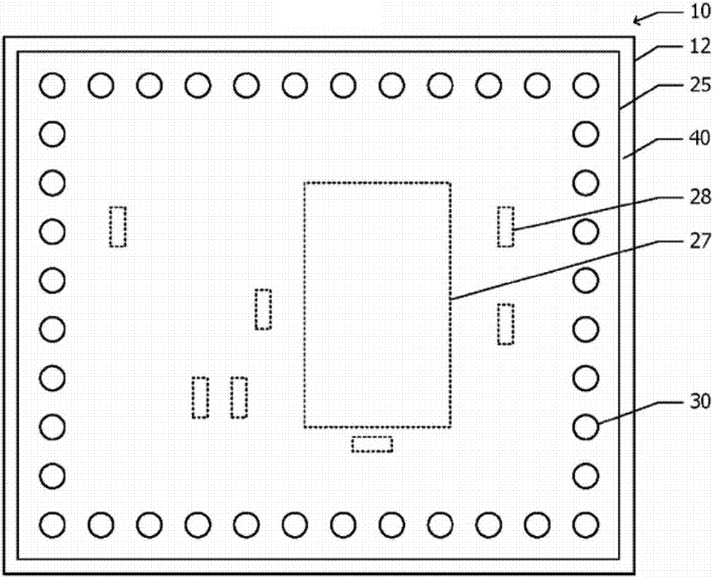
[0088] Reference Figure 7A as well as Figure 7B , The antenna module according to the third embodiment will be described. Below, the comparison with Figure 1 to Figure 4 The illustrated difference of the antenna module 10 according to Embodiment 1 will be described, and the description of the common structure will be omitted. In Example 3, a frame-shaped substrate 26 was used instead of the sealing resin layer 25 of Example 1 ( Figure 2A , Figure 2B ).

[0089] Figure 7A A bottom view of the antenna module 10 according to the third embodiment is shown. Figure 7B Means Figure 7A The cross-sectional view of the dotted line 7B-7B. A frame-shaped substrate 26 is bonded to the bottom surface of the dielectric substrate 12. A high-frequency semiconductor element 27 and a high-frequency circuit component 28 are mounted in an area surrounded by the frame-shaped substrate 26. The outer circumference of the frame-shaped substrate 26 is located slightly inside the outer circumfere...


PUM


Abstract

The invention discloses an antenna module and a circuit module. Disclosed is an antenna module wherein an antenna configured from a conductor pattern is disposed on a dielectric substrate. A high frequency semiconductor element is mounted on the bottom surface of the dielectric substrate, said high frequency semiconductor element supplying the antenna with high frequency signals. A plurality of conductor columns are protruding from the bottom surface. The conductor columns are embedded in a dielectric member disposed on the bottom surface. Leading ends of the conductor columns are exposed from the dielectric member. The dielectric member defines a mounting surface that faces a mounting substrate. A step is provided in a side surface of a composite structure configured from the dielectric substrate and the dielectric member, and the side surface from the mounting surface to the step is retracted from the side surface above the step. The antenna module, which is not susceptible to generating variance in radiation characteristics of the antenna even in a state wherein the antenna is bonded by means of a bonding resin, is provided.

Description

Technical field [0001] The present invention relates to an antenna module and a circuit module mounted on a mounting substrate. Background technique [0002] Patent Document 1 below discloses a multilayer module using a ceramic multilayer substrate. For the production of the ceramic multilayer substrate, for example, a ceramic green sheet cut into a square shape of 100 mm in length and 100 mm in width is used. Mount circuit components such as chip capacitors and chip resistors on ceramic multilayer substrates. A surface conductor is formed on one surface of the ceramic multilayer substrate. The multilayer module is mounted on the mounting substrate in a posture in which the surface on which the surface conductor is formed faces the mounting substrate. [0003] Although not described in Patent Document 1, the ceramic multilayer substrate on which chip capacitors and the like are mounted is cut into multiple multilayer modules. [0004] Patent Document 1: Japanese Patent Applicatio...

Claims


Application Information

Patent Timeline
Patent Type & Authority Applications(China)
IPC IPC(8): H01Q23/00H01L23/28H01Q1/24H01Q21/06H05K1/14
CPCH01L2924/181H01L2224/16225H01L2924/0002H01L21/561H01Q19/30H01Q21/065H01Q21/067H01Q25/00H01L23/3121H01L25/16H01L23/66H01L2223/6677H01L24/97H01L24/16H01L2924/15322H01L2924/15174H01L2924/00014H01L24/81H01L2224/97H01L2924/3025H01Q1/2283H01Q21/28H01L2924/19042H01L2924/19041H01L2924/19105H01L23/552H01L2924/15192H01L2924/00012H01L2224/13099H01L2224/81H01Q1/24H01Q23/00H01L21/78H01L23/3135H01L2223/6616H01L2224/16265H01L2924/19104H01Q1/38H01Q1/526H01Q21/22
Inventor 横山通春天知伸充
Owner MURATA MFG CO LTD
Why Eureka
Try Eureka