Inductor component and method for producing same

A technology of inductance components and manufacturing methods, applied in the direction of electrical components, inductance/transformer/magnet manufacturing, including printed electrical components, etc., can solve problems such as easy peeling of electroplating

Active Publication Date: 2018-03-27
MURATA MFG CO LTD
View PDF5 Cites 2 Cited by
  • Summary
  • Abstract
  • Description
  • Claims
  • Application Information

AI Technical Summary

Problems solved by technology

However, the plating formed on the resin layer has the problem of easy peeling

Method used


Image

  • Inductor component and method for producing same
  • Inductor component and method for producing same
  • Inductor component and method for producing same

Examples


no. 1 approach

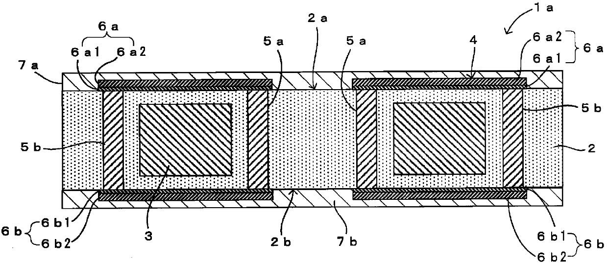
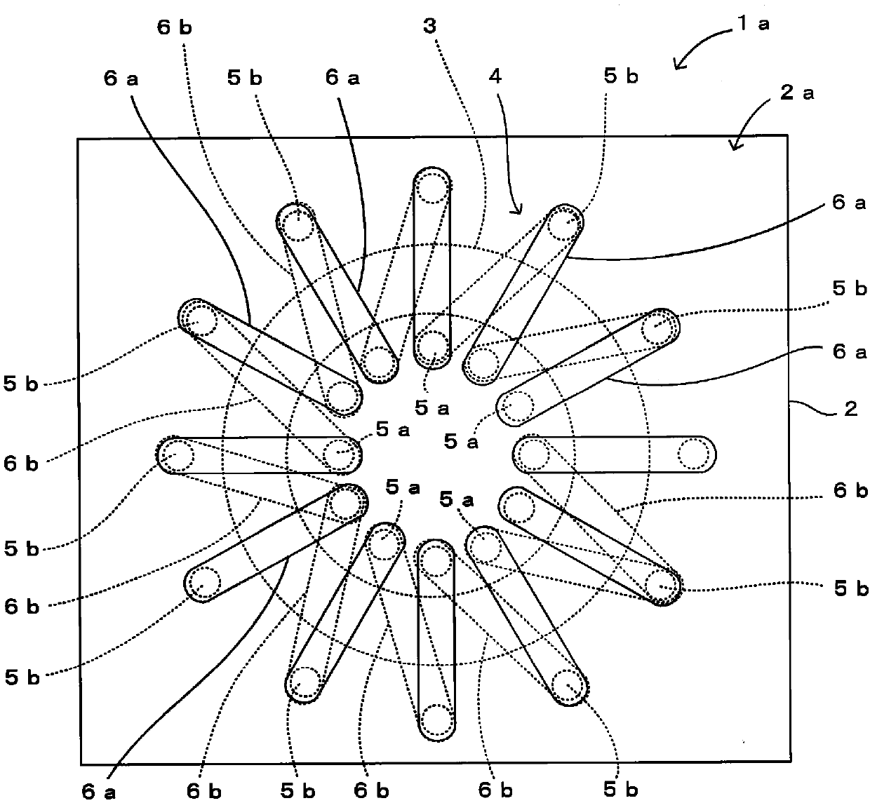
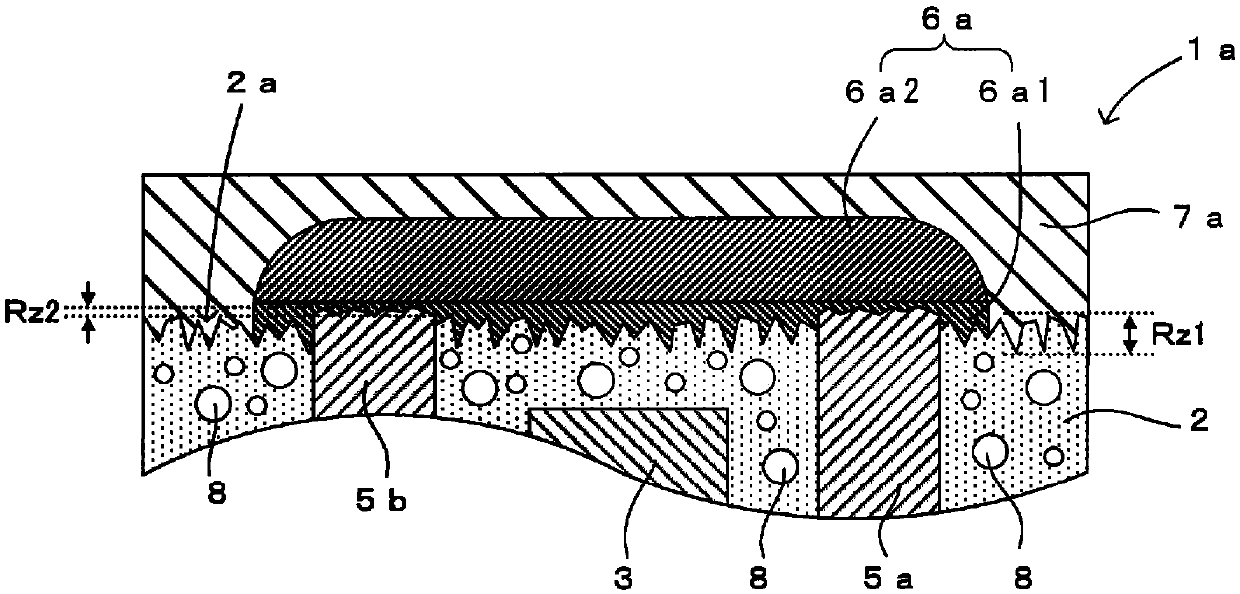
[0040] refer to Figure 1 to Figure 3 The inductance element according to the first embodiment of the present invention will be described. in addition, figure 1 is the cross-sectional view of the inductor element, figure 2 is the top view of the inductor element, image 3 is a partial cross-sectional view of the inductance element. In addition, in figure 2 In , illustration of the insulating coating films 7a and 7b is omitted.

[0041] Such as Figure 1 ~ Figure 3 As shown, the inductance element 1a of this embodiment includes: a resin layer 2 in which a coil core 3 is embedded; Around the ring core 3, the inductance element 1a is mounted on electronic devices such as mobile phones that use high-frequency signals.

[0042] The resin layer 2 is formed of a resin such as epoxy resin, for example, and is provided with a coil core 3 and a plurality of metal pins 5a, 5b which will be described later. In addition, in this embodiment, the resin layer 2 is formed of the epo...

no. 2 approach

[0067] refer to Figure 4 An inductance element according to a second embodiment of the present invention will be described. in addition, Figure 4 is a partial cross-sectional view of the inductance element, which is the same as image 3 corresponding figure.

[0068] Such as Figure 4 As shown, the inductance element 1b of this embodiment and the reference Figure 1 ~ Figure 3 The inductance element 1a of the first embodiment described is different in that the structures of the wiring patterns 6a and 6b are different. The other structures are the same as those of the inductance element 1a of the first embodiment, and therefore description thereof will be omitted by denoting the same reference numerals.

[0069] In this case, as Figure 4 As shown, each wiring pattern 6a, 6b has a cross-sectional shape in a direction perpendicular to the main surface of the resin layer 2 (upper surface 2a or lower surface 2b) expanding away from the main surface of the resin layer 2. T...

no. 3 approach

[0080] refer to Image 6 An inductance element according to a third embodiment of the present invention will be described. in addition, Image 6 is a partial cross-sectional view of the inductance element, which is the same as image 3 corresponding figure.

[0081] Such as Image 6 As shown, the inductance element 1c of this embodiment and the reference Figure 1 ~ Figure 3 The inductance element 1a of the first embodiment described is different in that the formation method of each of the wiring patterns 6a and 6b is different. The other structures are the same as those of the inductance element 1a of the first embodiment, and therefore description thereof will be omitted by denoting the same reference numerals. In addition, below, the manufacturing method of the inductance element 1c is demonstrated.

[0082] (Manufacturing method of inductance element 1c)

[0083] In this case, the process before grinding or grinding the upper surface 2a and the lower surface 2b of t...


PUM


Abstract

Provided is an inductor component having excellent characteristics and environmental reliability. This inductor component 1a is provided with a coil electrode 4 which comprises: a plurality of metal pins 5a, 5b having upper end faces exposed from the upper surface of a resin layer 2 and lower end faces exposed from the lower surface 2b of the resin layer 2; and a plurality of wiring patterns 6a, 6b that respectively connect the upper end faces or the lower end faces of specific metal pins 5a, 5b with each other. The surface roughness Rz1 of the upper surface 2a and the lower surface 2b of theresin layer 2 is rougher than the surface roughness of the upper end faces and the lower end faces of the metal pins. The wiring patterns 6a, 6b are formed by plating on the upper and lower surfaces 2a, 2b of the resin layer 2.

Description

technical field [0001] The present invention relates to an inductance element including a resin layer and an inductance electrode and a manufacturing method thereof. Background technique [0002] In electronic equipment that uses high-frequency signals, inductance elements are sometimes used as elements for preventing noise. In such an element, an inductor electrode may be constituted by a columnar conductor standing upright on the resin layer and a wiring electrode formed on the surface of the resin layer. In this case, the columnar conductors are formed by via conductors, metal pins, and the like, and the wiring electrodes are formed by, for example, printed patterns using conductive paste. In order to improve the characteristics by suppressing the impedance value of the inductor electrodes low, a technique of forming wiring electrodes by plating has been studied in recent years. Since the plated film contains less non-metallic components such as organic solvents like co...

Claims


Application Information

Patent Timeline
Patent Type & Authority Applications(China)
IPC IPC(8): H01F17/00H01F17/04H01F41/04H05K1/16
CPCH01F17/0013H01F17/062H01F41/041H05K1/16H01F27/24H01F27/2804H01F27/29H01F2027/2809
Inventor 水白雅章
Owner MURATA MFG CO LTD
Why Eureka
Try Eureka