Device and method for detecting semiconductor defects by exciting photoluminescence with dual light sources
A technology of photoluminescence and detection method, which is applied in the field of semiconductor material defect detection, and can solve problems such as inability to obtain deep energy level defects.
- Summary
- Abstract
- Description
- Claims
- Application Information
AI Technical Summary
Problems solved by technology
Method used
Image


Examples
Embodiment Construction
[0022] The present invention will be further described in detail in conjunction with the following specific embodiments and accompanying drawings. The process, conditions, experimental methods, etc. for implementing the present invention, except for the content specifically mentioned below, are common knowledge and common knowledge in this field, and the present invention has no special limitation content.
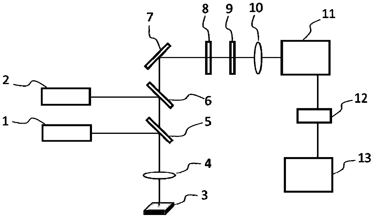
[0023] see figure 1 , the dual light source excitation photoluminescence detection semiconductor deep level defect detection device of the present invention comprises: a first laser light source 1, a second laser light source 2, a semiconductor sample 3, a first lens 4, a first beam splitter 5, a second beam splitter Sheet 6, mirror 7, first filter 8, second filter 9, second lens 10, monochromator 11, photodetector 12 and computer 13. The first laser light source 1 is focused to the surface of the semiconductor sample 3 through the first beam splitter 5 to the first lens ...
PUM
| Property | Measurement | Unit |
|---|---|---|
| wavelength | aaaaa | aaaaa |
Abstract
Description
Claims
Application Information