Compensation method and device for organic light emitting display panel

A technology of light-emitting display and compensation device, which can be applied to static indicators, instruments, etc., and can solve problems such as screen crosstalk and affecting screen display effects.

Active Publication Date: 2017-08-29
BOE TECH GRP CO LTD
View PDF7 Cites 11 Cited by
  • Summary
  • Abstract
  • Description
  • Claims
  • Application Information

AI Technical Summary

Problems solved by technology

[0003] Embodiments of the present invention provide a compensation method, a compensation device, and an organic light-emitting display device for an organic light-emitting display panel, which are used to solve the problem of the change in the v

Method used


Image

  • Compensation method and device for organic light emitting display panel
  • Compensation method and device for organic light emitting display panel
  • Compensation method and device for organic light emitting display panel

Examples


Embodiment 1

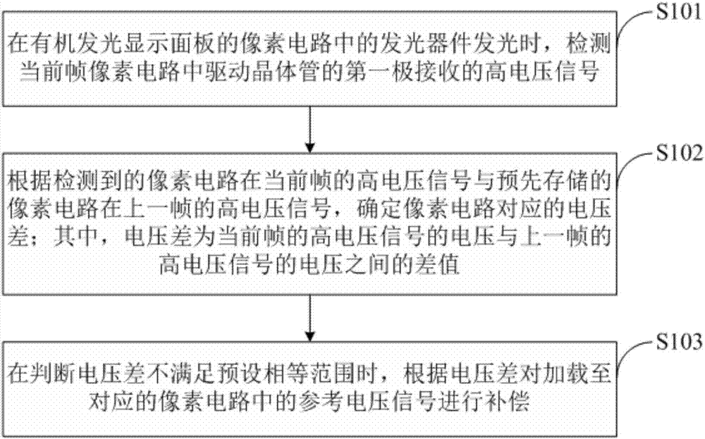
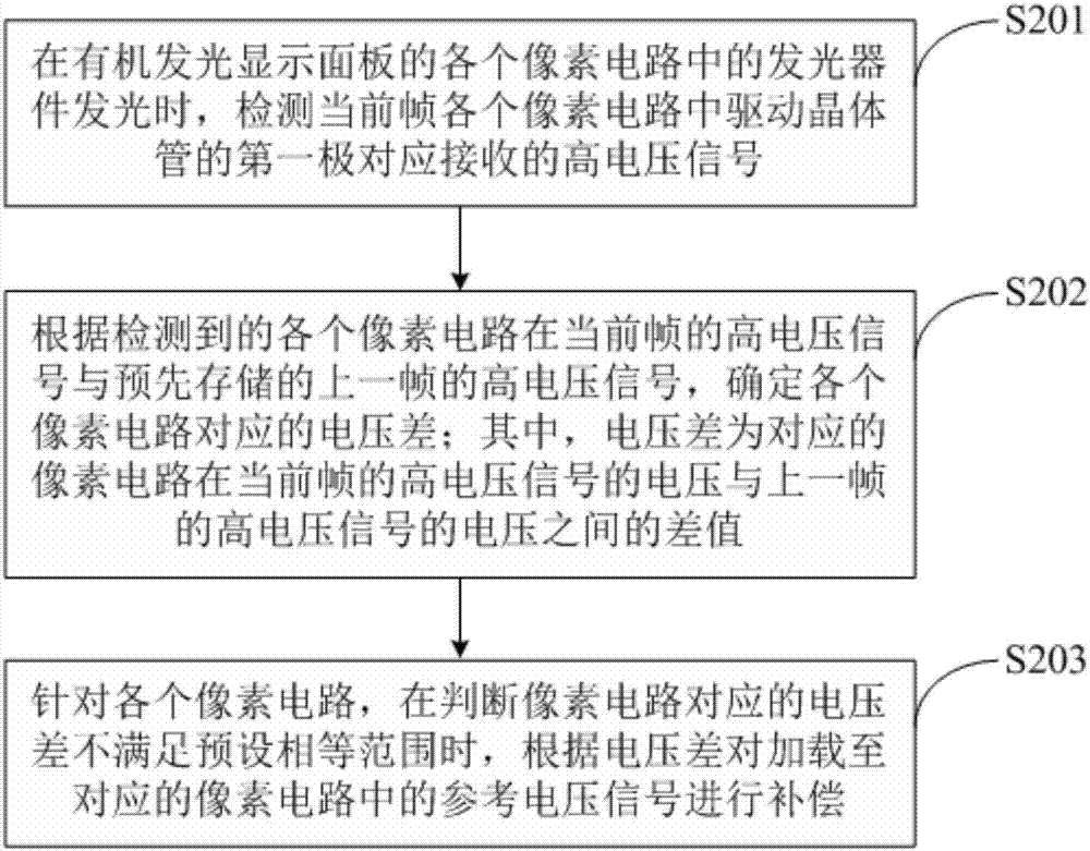
[0065] In an organic light-emitting display panel, the component that generally generates a high-voltage signal is the VDD power supply. Since the VDD power supply is connected to each pixel circuit in the organic light-emitting display panel through a signal line, and the signal line has a resistor, each pixel circuit receives All high voltage signals will have IR Drop. In the specific implementation, in the above method provided by the embodiment of the present invention, the display area of ​​the organic light emitting display panel may include a plurality of pixel circuits; figure 2 As shown, the compensation method may specifically include the following steps:

[0066] S201. When a light emitting device in each pixel circuit of an organic light emitting display panel emits light, detect a high voltage signal correspondingly received by a first electrode of a driving transistor in each pixel circuit of a current frame.

[0067] S202. According to the detected high-voltage...

Embodiment 2

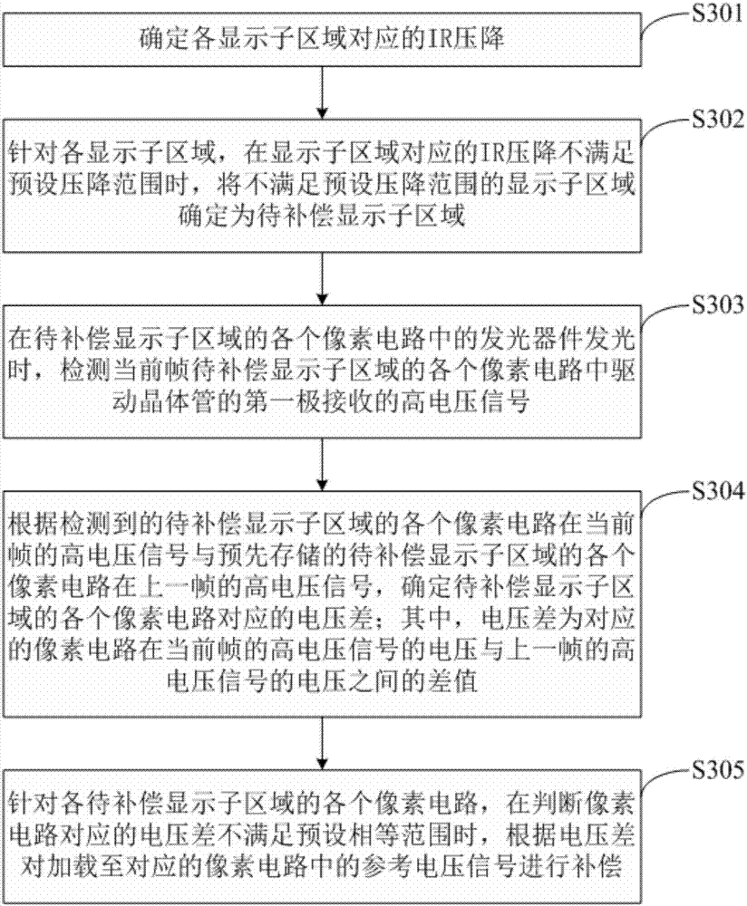
[0072] In an organic light-emitting display panel, the IR Drop corresponding to the pixel circuit closer to the VDD power supply may be smaller, and the IR Drop corresponding to the pixel circuit farther from the VDD power supply may be larger, and the pixel circuit corresponding to a smaller IR Drop When the high-voltage signal changes in two adjacent frames, the impact on the display effect of the screen may be small, or even negligible. Therefore, the pixel circuit for the small area of ​​IR drop does not need to be compensated, so that the power consumption can be further reduced.

[0073] In specific implementation, in the above-mentioned method provided by the embodiment of the present invention, the display area of ​​the organic light-emitting display panel may include a plurality of display sub-areas, and each display sub-area includes at least one pixel circuit; Before the first pole receives the high voltage signal, the compensation method may also include:

[0074]...

Embodiment 3

[0090] A general pixel circuit has various structures. In the specific implementation, in the above-mentioned method provided by the embodiment of the present invention, such as Figure 4 As shown, the pixel circuit may specifically include: a drive transistor M0, a storage capacitor Cst, a first switch transistor M1, a second switch transistor M2, a third switch transistor M3, a fourth switch transistor M4, a fifth switch transistor M5, and a sixth switch transistor. Transistor M6, wherein;

[0091] The first pole of the driving transistor M0 is used to receive the high voltage signal VDD, the second pole of the driving transistor M0 is connected to the first end of the light emitting device L through the sixth switching transistor T6; the second end of the light emitting device L is used to receive the low voltage Signal VSS.

[0092] The first pole of the first switching transistor M1 is used to receive the reference voltage signal Vref, the control pole of the first switc...


PUM


Abstract

The invention discloses a compensation method and device for an organic light emitting display panel, and an organic light emitting display panel. When a light emitting device in a pixel circuit in the current frame emits light, the high voltage signal received by a first pole of a driving transistor in the pixel circuit in the current frame is detected, wherein the high voltage signal is a signal which the driving transistor in the current frame is used for generating current to drive the connected light emitting device. Then the voltage difference between the high voltage signals received in the current frame and the previous frame by the driving transistor is determined based on the detected high voltage signal of the current frame in the pixel circuit and the pre-stored high voltage signal of the previous frame in the pixel circuit. A reference voltage signal applied to the pixel circuit is compensated based on the voltage difference when it is judged that the voltage difference does not satisfy the preset equal range, thereby solving the problem that the user is touching the moving picture to cause crosstalk of the screen, and further improving the screen display effect.

Description

technical field [0001] The invention relates to the field of display technology, in particular to a compensation method, a compensation device and an organic light-emitting display panel for an organic light-emitting display panel. Background technique [0002] Organic Light-Emitting Diode (OLED) is one of the hotspots in the field of flat panel display research today. Compared with Liquid Crystal Display (LCD), OLED has fast response, high brightness, high contrast, and low power consumption. As well as the advantages of easy realization of flexible display, it is considered to be the next generation mainstream display. Unlike LCD, which uses a stable voltage to control brightness, OLED is current-driven and requires a stable current to control light emission. At present, generally in OLED displays, the data signal Vdata is written into the gate of the driving transistor in the pixel circuit, and the high voltage signal VDD is input into the source of the driving transisto...

Claims


Application Information

Patent Timeline
IPC IPC(8): G09G3/3208
CPCG09G3/3208G09G2320/0209G09G3/3233G09G2300/0819G09G2320/0223
Inventor 玄明花
Owner BOE TECH GRP CO LTD
Why Eureka
Try Eureka