Electronic substrate and structure for connector connection thereof

a technology of electronic substrate and connector connection, applied in the direction of high frequency circuit adaptation, coupling device connection, printed circuit aspect, etc., can solve the problems of severe impedance mismatch to generate crosstalk, and influence caused by cross talk to become severe, so as to reduce parasitic capacitance and improve cross talk

Inactive Publication Date: 2016-08-30
NEC CORP
View PDF21 Cites 12 Cited by
  • Summary
  • Abstract
  • Description
  • Claims
  • Application Information

AI Technical Summary

Benefits of technology

[0015]According to the present invention, it is possible to reduce the parasitic capacitance which exists between the connection terminals, and consequently it is possible to improve the cross talk.

Problems solved by technology

Accordingly, there is a problem that capacitive coupling causes an impedance mismatch to generate crosstalk.
Moreover, as a cycle of digital signal becomes short, influence caused by the cross talk becomes severe.
Furthermore, as the parasitic capacitance of the connection terminal becomes large, the influence caused by the cross talk becomes severe.

Method used


Image

  • Electronic substrate and structure for connector connection thereof
  • Electronic substrate and structure for connector connection thereof
  • Electronic substrate and structure for connector connection thereof

Examples


example 1

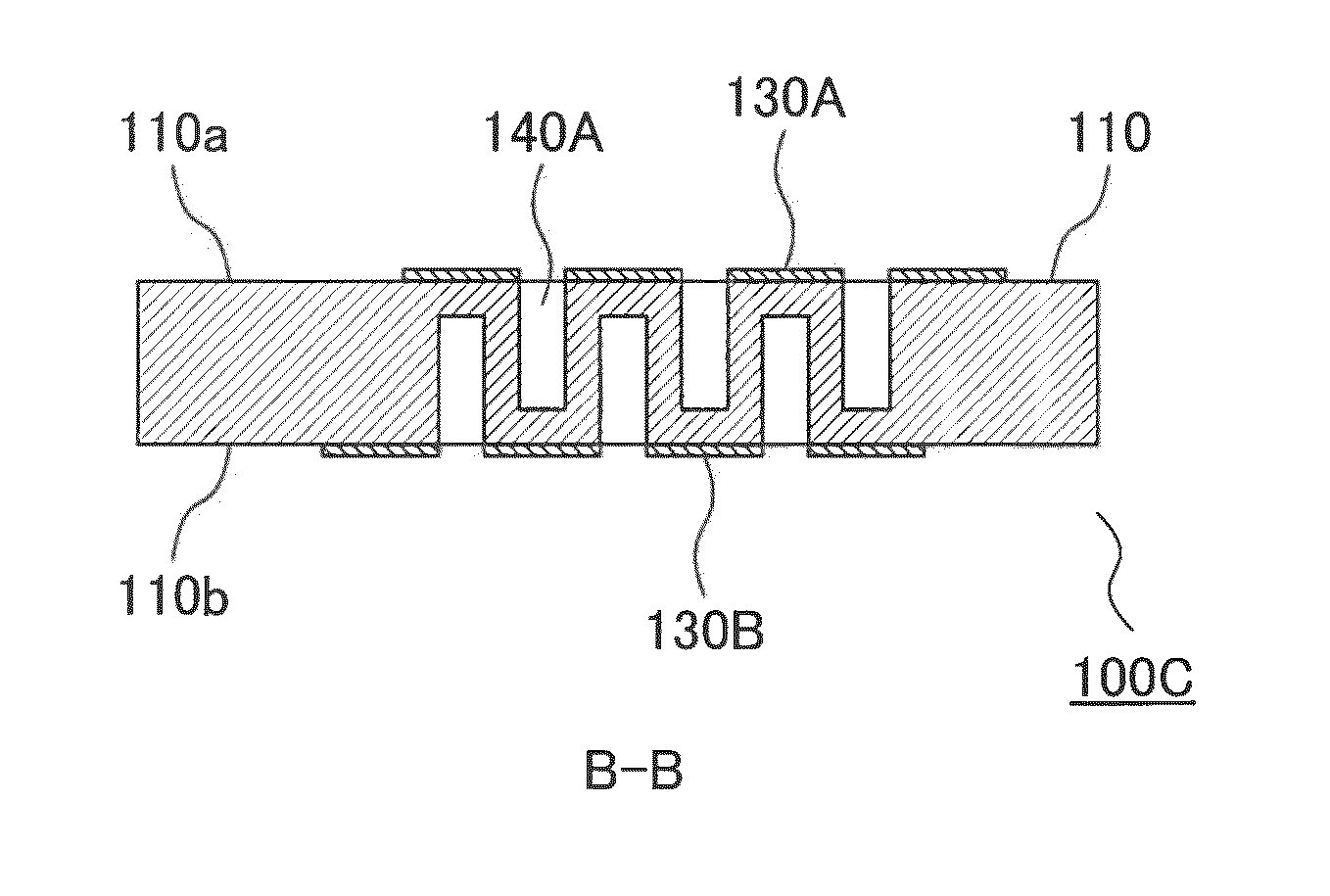
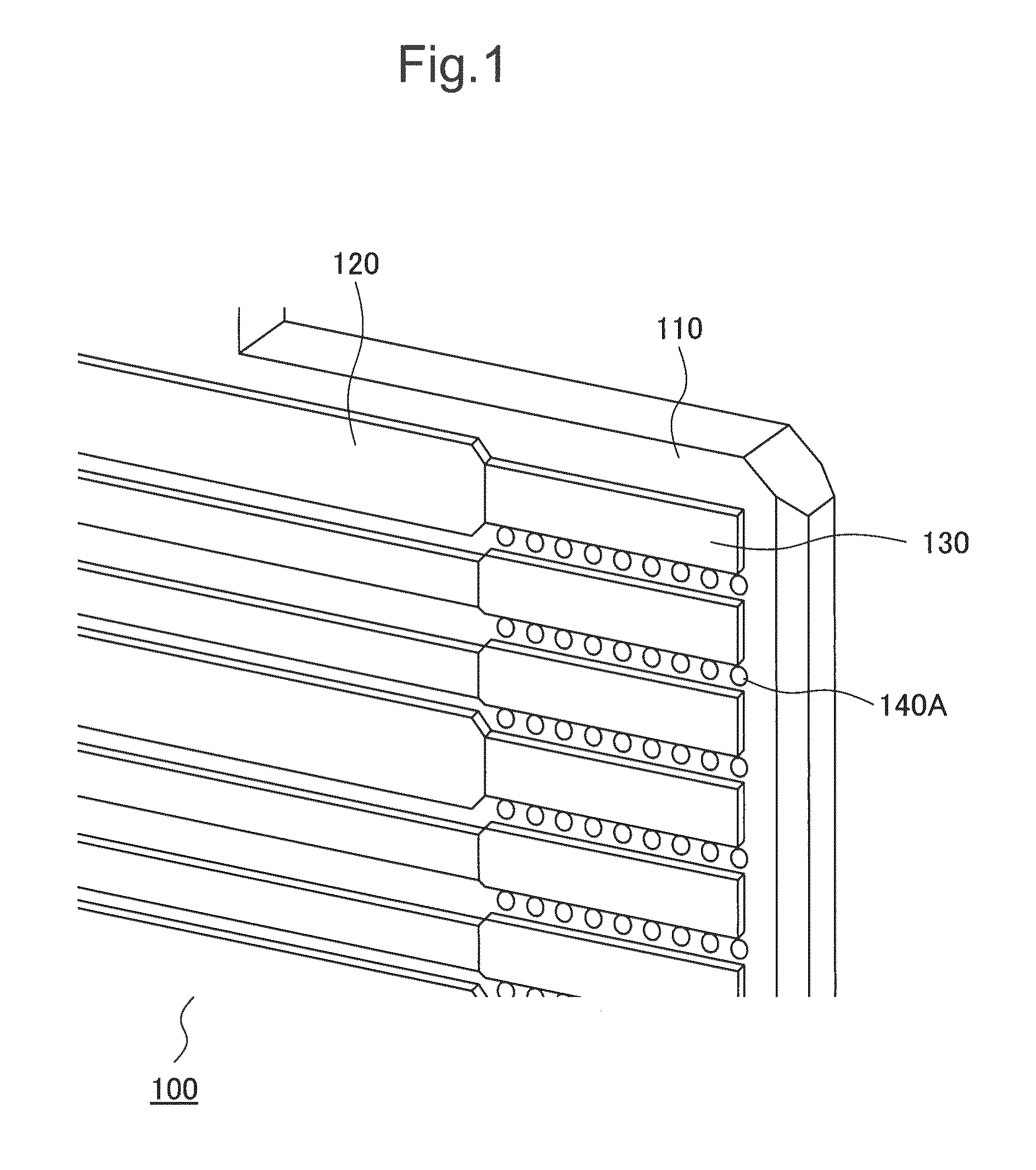
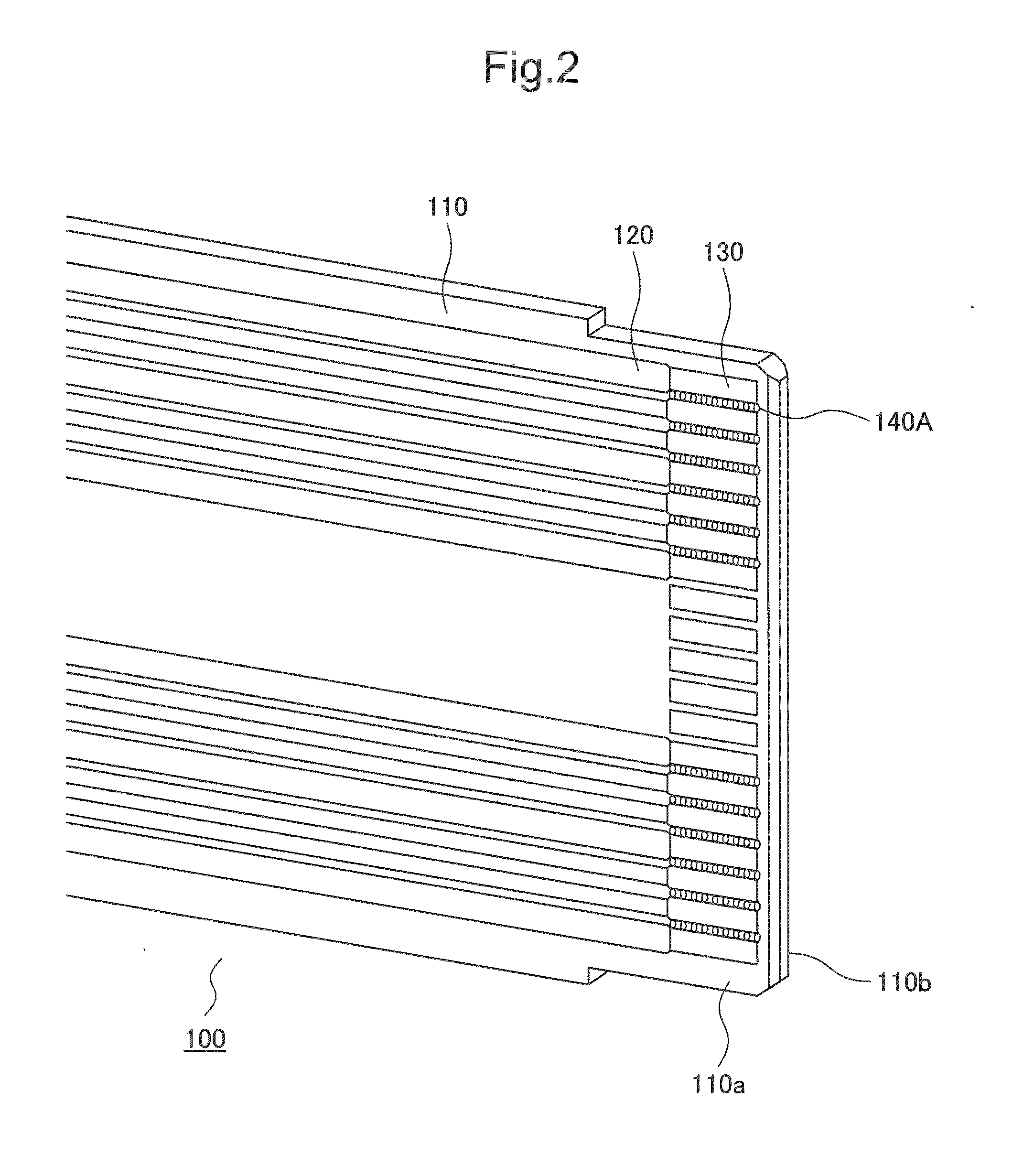
[0108]As mentioned above, the example 1 is corresponding to the electronic substrate 100D (refer to FIG. 8) in the fourth exemplary embodiment of the present invention. A glass epoxy member (relative permittivity is 3.8), whose thickness, that is, thickness between the pair of main surfaces 110a and 110b is 1 mm, is used as the substrate member 110. A connection terminal, which is made of the gold plating copper alloy and whose length of a short side is 0.6 mm and whose thickness is 43 μm, is used as the first connection terminal 130A and the second connection terminal 130B. A distance between one connection terminal and another connection terminal, which is adjacent to the one connection terminal, is set to be 0.2 mm. The opening 140B is set so as to have a shape of rectangle whose length of a long side is 2.25 mm and whose length of a short side is 0.15 mm, and to have a depth of 0.58 mm.

example 2

[0109]As mentioned above, the example 2 is corresponding to the electronic substrate 100C (refer to FIG. 7A and FIG. 7B) in the fourth exemplary embodiment of the present invention. In comparison with the example 1, the example 2 is different from the example 1 in a point that the plural openings 140A are arranged in the example 2 in place of the opening 140B having the shape of rectangle which is used in the example 1. Each of the plural openings 140A is set so as to have a diameter of 0.15 mm, and a depth of 0.58 mm. Another condition is the same as one of the example 1.


PUM


Abstract

An electronic substrate 100 includes: a substrate member 110 which has a shape of plane plate and whose pair of main surfaces 110a and 110b are opposite each other; a plurality of connection terminals 130 which are formed so as to be arranged on an edge side of the substrate member 110 and on at least one surface out of the pair of main surfaces 110a and 110b of the substrate member 110; a plurality of wirings 120 which are connected with the plural connection terminals 130; and a plurality of openings 140A arranged in an area, which exists between connection terminals 130 adjacent each other out of the plural connection terminals 130 and in which the connection terminals 130 adjacent each other extend, in an extending direction of the connection terminals 130 adjacent each other.

Description

TECHNICAL FIELD[0001]The present invention relates to an electronic substrate and the like, and, for example, relates to an electronic substrate, which has a plurality of connection terminals arranged on an edge of a substrate member, or the like.BACKGROUND ART[0002]Recently, an art to connect an electronic substrate, which has a shape of plane plate and at whose edge a connection terminal is arranged, and a connector electrically by inserting the electronic substrate into a slot of the connector is well-known.[0003]The electronic substrate, which is used in the above-mentioned art, has structure shown, for example, in FIG. 13 and FIG. 14. A wiring 120, which is used as a signal line, is arranged on a substrate member 110 which has a shape of plane plate. The wiring 120 is connected with a connection terminal 130 which is arranged on an edge side of the substrate member 110. A transmission signal is transmitted from the wiring 120 to the connection terminal 130. Moreover, a signal i...

Claims


Application Information

Patent Timeline
Patent Type & Authority Patents(United States)
IPC IPC(8): H05K1/11H01R12/72H01R13/6473H01R13/6461H05K1/02H01R12/73
CPCH01R12/721H05K1/025H05K1/117H01R13/6461H01R13/6473H01R12/73H05K1/024H05K2201/0191H05K2201/09036H05K2201/09709
Inventor KASHIWAKURA, KAZUHIRO
Owner NEC CORP
Why Eureka
Try Eureka