Chip encapsulation structure and circuit structure

A chip packaging structure and chip technology, applied in circuits, electrical components, electrical solid devices, etc., can solve the problems of low chip packaging efficiency, complex process, complex chip packaging process, etc. Simple packaging process

Inactive Publication Date: 2017-08-29
HUAWEI TECH CO LTD
View PDF4 Cites 18 Cited by
  • Summary
  • Abstract
  • Description
  • Claims
  • Application Information

AI Technical Summary

Problems solved by technology

[0004] However, in the above process, due to the complicated process of TSV technology, the chip packaging process is complicated, resulting in low efficiency of chip packaging

Method used


Image

  • Chip encapsulation structure and circuit structure
  • Chip encapsulation structure and circuit structure
  • Chip encapsulation structure and circuit structure

Examples


Embodiment Construction

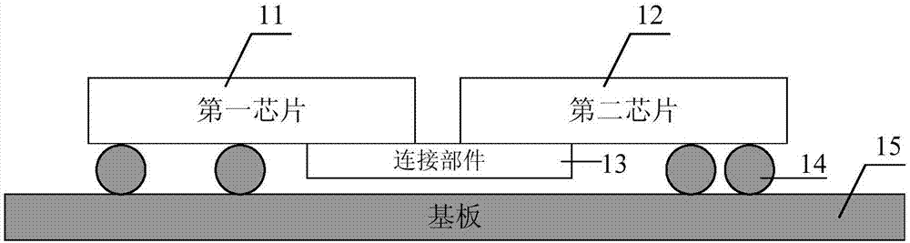
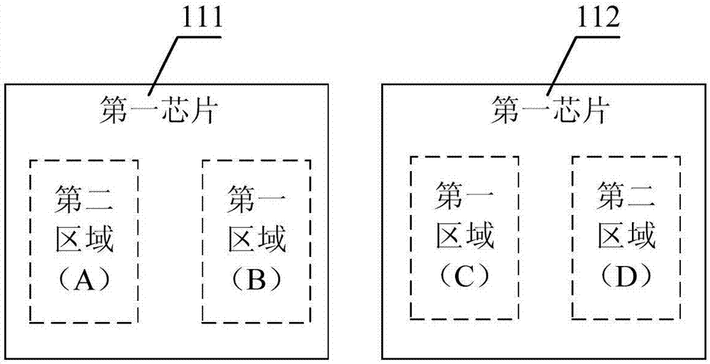
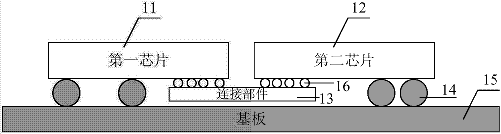
[0097] The chip packaging structure involved in the present application includes at least two chips, and the at least two chips are connected to each other so as to realize mutual communication between the chips. Optionally, the chips shown in this application may be logic chips or memory chips. The chip packaging structure shown in this application aims to simplify the chip packaging process and improve the chip packaging efficiency.

[0098] In the following, the chip packaging structure described in this application will be described in detail through specific embodiments. It should be noted that the following specific embodiments may be combined with each other, and the same or similar content will not be repeated in different embodiments. It should also be noted that the lengths, widths, and heights (or thicknesses) of various components shown in the drawings of this application are only illustrative, and not limiting to the chip packaging structure described in this app...


PUM


Abstract

The invention provides a chip encapsulation structure and a circuit structure. The chip encapsulation structure comprises at least two chips, a connection part, multiple second welding balls and a substrate; the active surface of each chip in the at least two chips is positioned in the same plane; the active surface of each chip comprises a first area and a second area; multiple first bonding pads are arranged in the first area; at least one second bonding pad is arranged in the second area; the at least two chips comprise a first chip and a second chip, which are adjacent; multiple first metal wires are distributed in the connection part; both two ends of each first metal wire are exposed on the first surface of the connection part; one end of each first metal wire is connected with one first bonding pad of the first chip; the other end of each first metal wire is connected with one first bonding pad of the second chip; each second bonding pad of the first chip and the second chip is connected with the upper surface of the substrate through a second welding ball; and the upper surface of the substrate is towards the active surface of the chip. By means of the chip encapsulation structure and the circuit structure provided by the invention, the chip encapsulation efficiency is increased.

Description

technical field [0001] The present application relates to the technical field of chip packaging, in particular to a chip packaging structure and a circuit structure. Background technique [0002] As the amount of data to be transmitted between chips increases, more and more connecting wires between chips are required. Since the volume of the chip is small, and the packaging volume of the chip cannot be too large, a relatively high process is required to realize the connection between the chips. [0003] At present, the interconnection between multiple chips is generally realized by a technology of disposing a wafer on a substrate and stacking chips on the wafer (Chip on Wafer on Substrate, CoWoS). Specifically, a plurality of chips are arranged on the upper surface of the adapter board. Since the upper surface of the adapter board is provided with metal wiring, the plurality of chips can be interconnected through the metal wiring on the upper surface of the adapter board. ...

Claims


Application Information

Patent Timeline
Patent Type & Authority Applications(China)
IPC IPC(8): H01L25/065H01L25/18H01L23/538H01L21/98
CPCH01L23/538H01L25/0655H01L25/18H01L25/50H01L2224/18H01L2224/96H01L2224/16227H01L2924/15192H01L2224/1703H01L2924/18162H01L2224/12105H01L2224/73209H01L24/19H01L24/96H01L2924/15311H01L2924/16251H01L2224/16145H01L2224/73267H01L2224/32245
Inventor 张童龙谢荣华张峰
Owner HUAWEI TECH CO LTD
Why Eureka
Try Eureka