Methods of Fabrication and Testing of Three-Dimensional Stacked Integrated Circuit System-In-Package

a technology of integrated circuit system and three-dimensional stack, which is applied in the direction of individual semiconductor device testing, semiconductor/solid-state device testing/measurement, instruments, etc., can solve the problems of high manufacturing cost, difficult process yield and cost, etc., and achieve low cost and high integration

Active Publication Date: 2015-10-29
NINGBO SEMICON INT CORP
View PDF13 Cites 19 Cited by
  • Summary
  • Abstract
  • Description
  • Claims
  • Application Information

AI Technical Summary

Benefits of technology

[0019]By bonding dielectric layers of a plurality of second dies sliced from a second semiconductor wafer to dielectric layers of a plurality of first dies on a first semiconductor wafer which serves as a carrier and interconnecting an exposed area of each second die and an exposed area of a corresponding first die by a plating process, the present invention enables the construction of 3D stacked systems of the first and second dies. In addition, the present invention also enables electronic testing of these stacked systems by bringing microprobes into contact with input / output bond pads overlying plating solder points formed on the first dies.
[0020]The fabrication and testing methods of the present invention allow wafer-level SiP fabrication, electrical interconnection and system testing and offers advantages such as process simplicity, high integration and low cost.

Problems solved by technology

However, the application of the solder-bump flip chip process using densely arranged solder bumps in 3D stacking and interconnection still remains a great challenge and leads to high manufacturing costs.
In particular, the void-free filling and reliable curing of a liquid medium within the gaps between the dies after the flipping and solder bump reflowing is a very challenging process to yield and cost issues.

Method used


Image

  • Methods of Fabrication and Testing of Three-Dimensional Stacked Integrated Circuit System-In-Package
  • Methods of Fabrication and Testing of Three-Dimensional Stacked Integrated Circuit System-In-Package
  • Methods of Fabrication and Testing of Three-Dimensional Stacked Integrated Circuit System-In-Package

Examples


embodiment 1

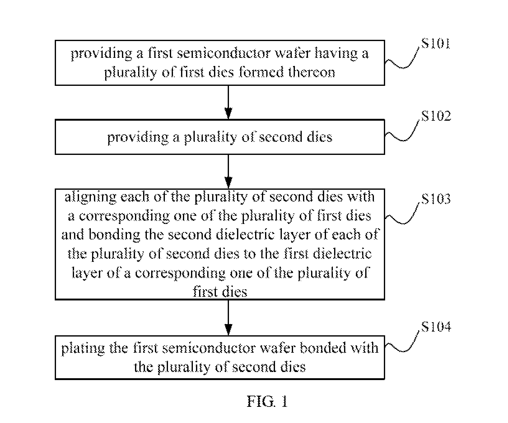
[0031]Referring to FIG. 1, in this embodiment, a method of fabricating a 3D stacked IC SiP includes the steps described in detail below.

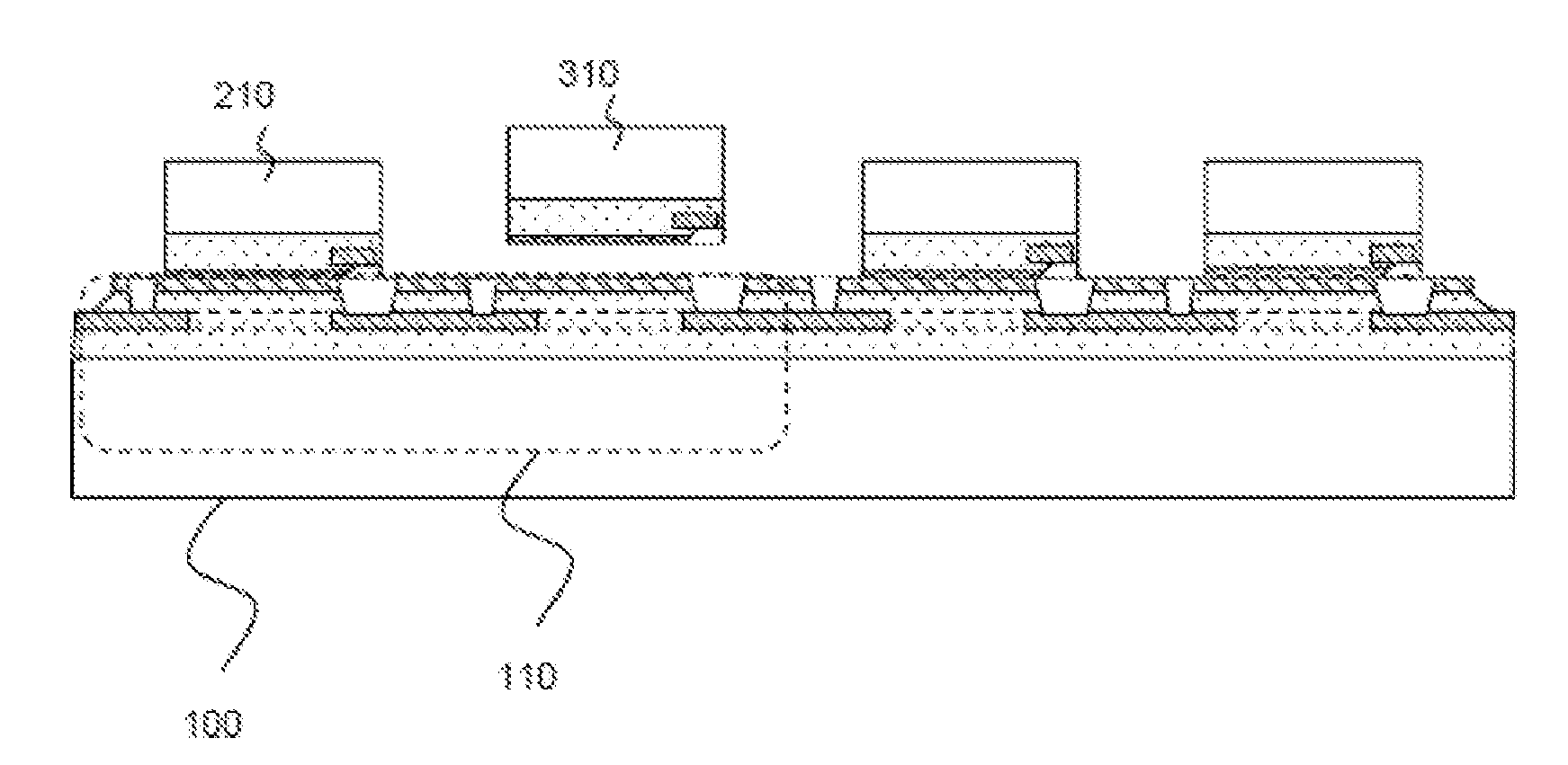
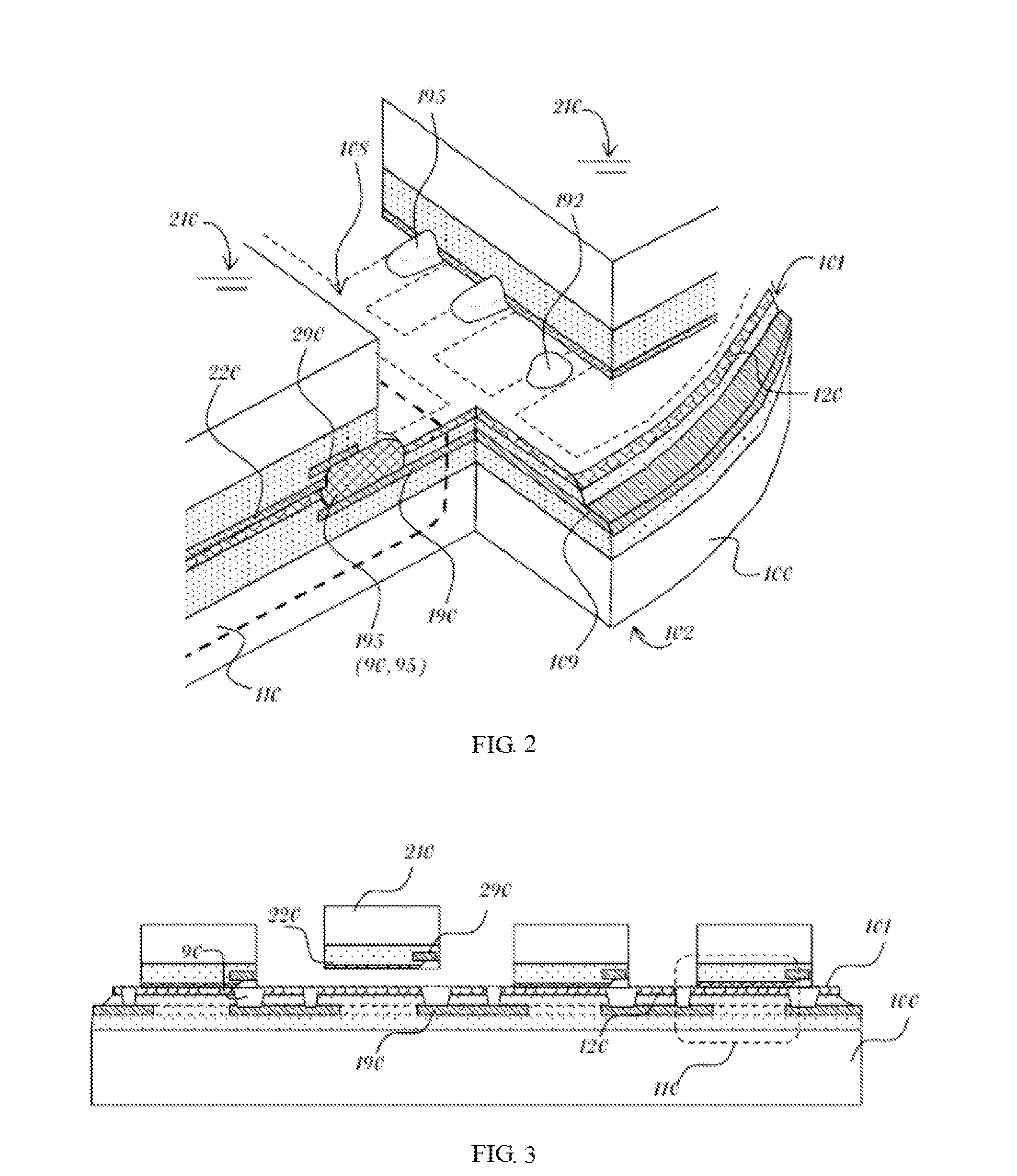
[0032]In step S101, as shown in FIGS. 2 and 3, a first semiconductor wafer 100 is provided, on which a plurality of first dies 110 are formed. The top surfaces of the plurality of first dies 110 are located in the same plane as a top surface of the first semiconductor wafer 100. Each first die 110 is provided with a first wire bond pad 190 formed in a peripheral part of the specific first die with at least a portion of the surface of the first wire bond pad 190 exposed in the air. A first dielectric layer 120 is formed over each first die 110 and covers the rest part of the surface of the specific first die 110 other than the exposed portion of the surface of the first wire bond pad 190. Specifically, in this embodiment, the first semiconductor wafer 100 is implemented as a silicon semiconductor substrate, and the first dielectric layer 120 is a cur...

embodiment 2

[0043]A method according to this embodiment has some steps that are the same as those of the method of Embodiment 1 and are thus not further described herein, except that step S103 of the method of this embodiment includes:

[0044]step S1031: arranging the individual second dies 210 at positions corresponding to the respective first dies 110, with the second dielectric layers 220 of the second dies 210 all located in the same plane, and injection molding a second wafer 200 by filling an injection molding material 209 among the second dies, as shown in FIGS. 2 and 8, and exposing portions of the second wire bond pads 290 by etching away the injection molding material 209 thereon, as shown in FIG. 9;

[0045]step S1032: vertically aligning the second wafer 200 with the first semiconductor wafer 100 such that each second die 210 on the second wafer 200 faces a corresponding one of the first dies 110 on the first semiconductor wafer 100, and bonding the second dielectric layer 220 on each se...

embodiment 3

[0050]A method according to this embodiment has some steps that are the same as those of the methods of the previous embodiments and are thus not further described herein, but there are some differences as described below.

[0051]In this embodiment, referring to FIG. 2, all the first wire bond pads 190 in the first dies 110 are electrically connected. Specifically, in this embodiment, an interconnection in the form of a conductive grid 109 including a conductive lead frame 108 is formed on the top surface of the first semiconductor wafer 100 and electrically connected with all the first wire bond pads 190 in the first dies 110, with the conductive lead frame 108 covering the periphery of the first semiconductor wafer.

[0052]In a chip fabrication process, a metal layer may be first deposited and etched to form desired interconnecting metal wires. Part of a dielectric layer formed over the surfaces of the dies may then be etched away to expose input / output terminals of the interconnectin...


PUM


Abstract

The present invention provides a method of fabricating a 3D stacked IC SiP which includes: providing a first semiconductor wafer having a plurality of first dies formed thereon, each having a first wire bond pad and a first dielectric layer, at least a portion of the first wire bond pad is not covered by the first dielectric layer and constitutes an exposed area of the first die; providing a plurality of second dies, each having a second wire bond pad and a second dielectric layer, at least a portion of the second wire bond pad is not covered by the second dielectric layer and constitutes an exposed area of the second die different in size from that of the first die; aligning the second dies with the first dies and bonding the second dielectric layer to the first dielectric layer; plating the first semiconductor wafer bonded with the second dies.

Description

CROSS-REFERENCES TO RELATED APPLICATIONS[0001]This application claims the priority of Chinese patent application number 201410168052.X, filed on Apr. 24, 2014, the entire contents of which are incorporated herein by reference.TECHNICAL FIELD[0002]The present invention provides methods of fabricating and testing a three-dimensional (3D) stacked integrated circuit (IC) system-in-package (SiP) and relates to the field of semiconductor system integration and packaging.BACKGROUND[0003]System-in-packages (SiPs) of various three-dimensional (3D) stacked architectures have found increasing use in the field of integrated circuit (IC) SiP testing. For example, a 3D SiP of the most typical type, i.e., an SiP containing two vertically stacked chips, can be formed by any of the following approaches:[0004]1) three-dimensionally attaching the two vertically stacked dies onto a substrate with a curing adhesive, and connecting contacts of the two dies to the substrate with wire bonds;[0005]2) three-...

Claims


Application Information

Patent Timeline
Patent Type & Authority Applications(United States)
IPC IPC(8): H01L25/00H01L23/00H01L21/66H01L21/56
CPCH01L25/50H01L22/14H01L24/83H01L21/565H01L21/76898H01L21/561H01L21/568H01L24/96H01L2224/16147H01L2224/92143H01L2224/0392H01L24/03H01L24/05H01L24/13H01L24/16H01L24/29H01L24/32H01L24/81H01L24/92H01L24/94H01L24/97H01L25/0657H01L2224/0401H01L2224/0557H01L2224/13139H01L2224/13147H01L2224/13155H01L2224/13157H01L2224/2919H01L2224/32145H01L2224/73204H01L2224/81002H01L2224/811H01L2224/83121H01L2224/83855H01L2224/83862H01L2224/83868H01L2224/83871H01L2224/83874H01L2224/92H01L2224/94H01L2224/96H01L2224/97H01L2225/06513H01L2225/06541H01L24/82H01L24/24H01L2224/24105H01L2224/24145H01L2224/24147H01L2224/82101H01L2224/82108H01L2224/92144H01L2224/73217H01L2924/00014H01L2924/00012H01L2924/01015H01L2924/01005H01L2224/81H01L2224/83H01L2224/03H01L21/56H01L21/78H01L21/304H01L2224/82H01L2224/16145H01L2924/00
Inventor MAO, JIANHONGHAN, FENGQINWANG, ZHIWEICHANG, WENFEN
Owner NINGBO SEMICON INT CORP
Why Eureka
Try Eureka