

Array substrate, display panel and display device
An array substrate and substrate technology, applied in nonlinear optics, instruments, optics, etc., can solve the problems of affecting display quality, difficult impedance matching, and large impedance difference between Metal1 and Metal2
- Summary
- Abstract
- Description
- Claims
- Application Information
AI Technical Summary
Problems solved by technology
Method used
Image

Examples
Embodiment Construction
[0033] The present invention will be further described in detail below in conjunction with the accompanying drawings and embodiments. It should be understood that the specific embodiments described here are only used to explain the present invention, but not to limit the present invention. In addition, it should be noted that, for the convenience of description, only some structures related to the present invention are shown in the drawings but not all structures.
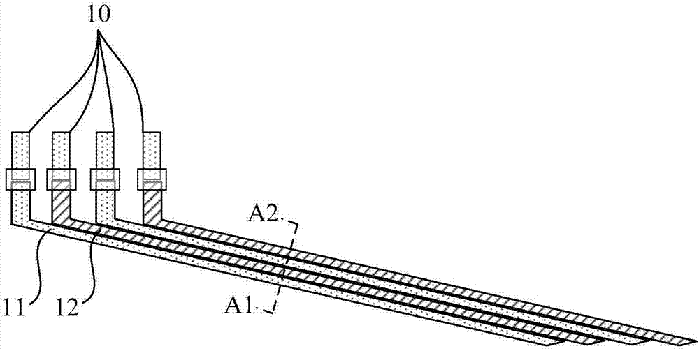
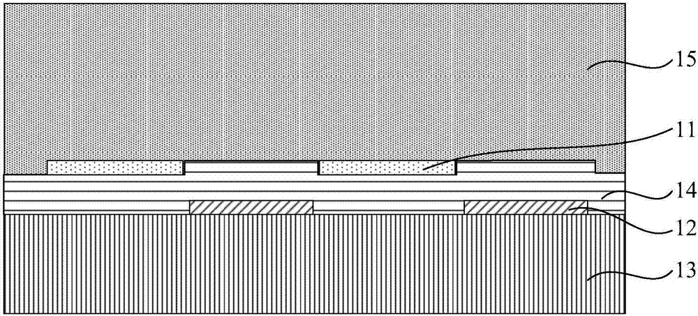
[0034] Figure 1a It is a schematic diagram of the plane structure of the existing fan-out routing layout; Figure 1b for Figure 1a Schematic diagram of the cross-sectional structure along A1-A2. The fan-out line is located in the non-display area of the display panel, adopts a two-layer metal fan-out line structure, and is electrically connected to a signal line (such as a data line, a gate line, and a touch line, etc.) in the display area of the display panel, such as Figure 1a with Figure 1b As shown, t...
PUM
 Abstract
Description
Claims
Application Information