
Display panel and manufacturing method thereof

A technology for display panels and substrates, used in semiconductor/solid-state device manufacturing, diodes, semiconductor devices, etc., can solve problems such as uneven display of self-luminous panels, affect display effect, color mixing, etc. effect, the effect of reducing negative effects

Inactive Publication Date: 2017-09-15
HKC CORP LTD +1
View PDF5 Cites 5 Cited by
  • Summary
  • Abstract
  • Description
  • Claims
  • Application Information

AI Technical Summary

Problems solved by technology

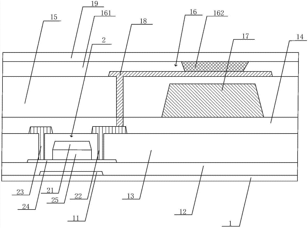
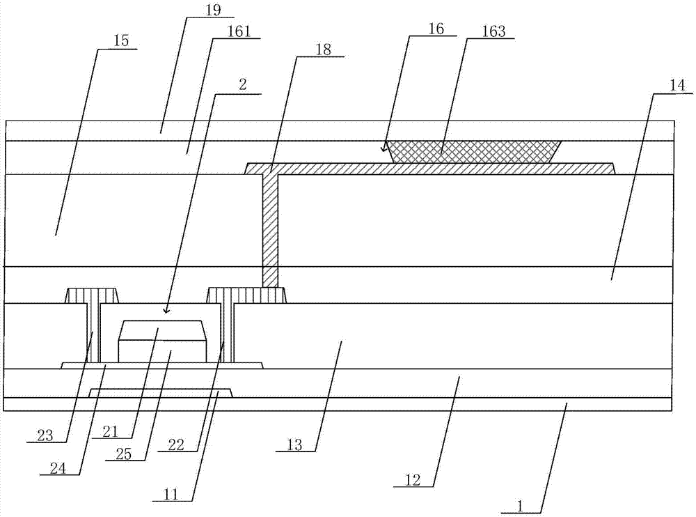
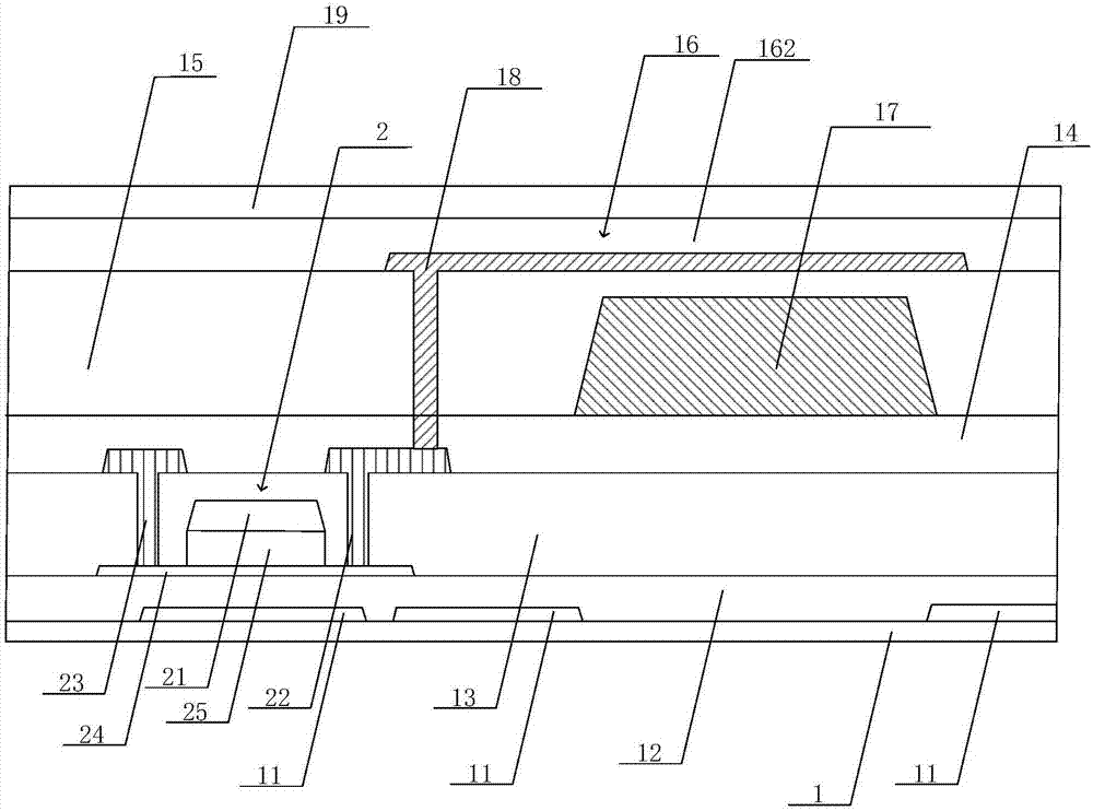
This traditional process has a large number of channels and the process is complex, but if the pixel definition layer is omitted, it will cause uneven display or color mixing of the self-luminous panel, which will affect the display effect

Method used


Image

  • Display panel and manufacturing method thereof
  • Display panel and manufacturing method thereof
  • Display panel and manufacturing method thereof

Examples


Embodiment Construction

[0057] The specific structure and functional details disclosed herein are only representative, and are used for the purpose of describing exemplary embodiments of the present invention. However, the present invention can be embodied in many alternative forms, and should not be construed as being limited only to the embodiments set forth herein.

[0058] In the description of the present invention, it should be understood that the terms "center", "lateral", "upper", "lower", "left", "right", "vertical", "horizontal", "top", The orientation or positional relationship indicated by "bottom", "inner", "outer", etc. are based on the orientation or positional relationship shown in the drawings, which is only for the convenience of describing the present invention and simplifying the description, and does not indicate or imply the pointed device Or the component must have a specific orientation, be constructed and operated in a specific orientation, and therefore cannot be understood as ...


PUM


Abstract

The invention discloses a display panel and a manufacturing method thereof. The manufacturing method comprises the steps of: providing a substrate; forming an active switch on the substrate; forming a light emitting layer on the active switch, and electrically connecting the light emitting layer to the active switch; forming a flat layer between the active switch and the light emitting layer, wherein the flat layer is provided with a through hole; and, filling a colourful photoresist layer in the through hole of the flat layer, wherein the colourful photoresist layer is aligned to the light emitting layer. Thereby, the display effect of a self-light-emitting display panel can be well ensured.

Description

Technical field [0001] The present invention relates to the field of display technology, and more specifically, to an organic light emitting diode display panel and a manufacturing method thereof. Background technique [0002] Active-matrix organic light emitting diode (AMOLED) display has the characteristics of high contrast, wide color gamut, and fast response speed. Because AMOLED is self-luminous and does not need a backlight, it can be made lighter, thinner and even more flexible than AMLCD. The AMOLED display screen is mainly controlled by a specific TFT to adjust the switch and brightness of the OLED device, and the screen is displayed after adjusting the ratio of the three primary colors. Among them, the control TFT often uses a metal oxide semiconductor, which not only has a higher on-state current and a lower off-state current, but also has the characteristics of higher uniformity and stability. [0003] After the anode manufacturing process, the pixel definition layer ...

Claims


Application Information

Patent Timeline
Patent Type & Authority Applications(China)
IPC IPC(8): H01L51/52H01L51/56H01L27/32
CPCH10K59/122H01L27/1225H10K59/38H10K59/124H10K59/126H10K50/85H10K71/00
Inventor 陈猷仁
Owner HKC CORP LTD
Learn More