

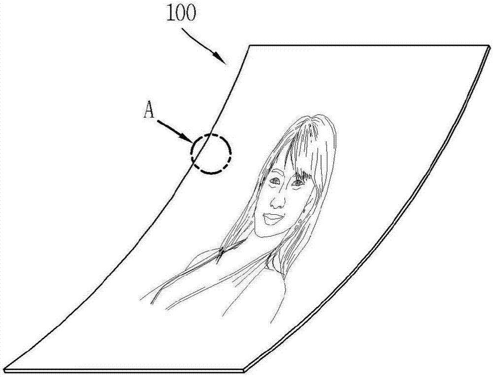
Display device using semiconductor light emitting device and method for manufacturing the same
一种显示装置、发光器件的技术,应用在半导体器件、电固体器件、照明装置等方向,能够解决存在限制、相关分隔壁结构的研究尚未进行、研究不充分等问题,达到提高效率、高分辨率、确保面积的效果
- Summary
- Abstract
- Description
- Claims
- Application Information
AI Technical Summary
Problems solved by technology
Method used
Image

Examples
Embodiment Construction
[0037] Hereinafter, embodiments disclosed herein will be described in detail with reference to the drawings, the same or similar elements are denoted by the same reference numerals regardless of the numerals in the drawings, and repeated descriptions thereof will be omitted. The suffix "module" or "unit" used by the constituent elements disclosed in the following description is only for simple description of the specification, and the suffix itself does not have any special meaning or function. Also, it should be noted that the accompanying drawings are shown only for easy explanation of the concept of the present invention, and thus, should not be construed as limiting the technical concept disclosed herein with the accompanying drawings.
[0038] In addition, when an element such as a layer, region or substrate is referred to as being "on" another element, it can be directly on the other element or intervening elements may also be interposed therebetween.
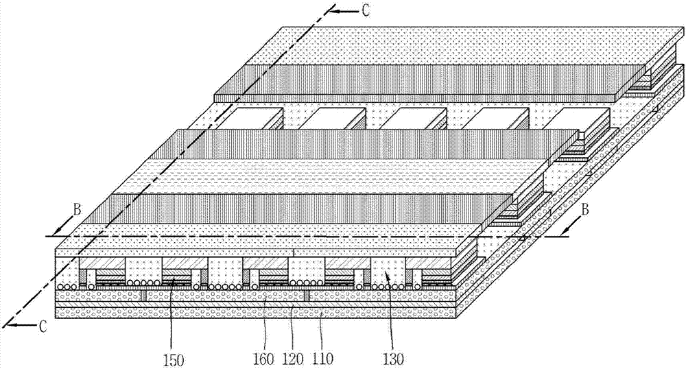
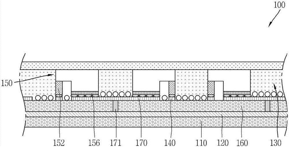
[0039] Display de...
PUM
 Abstract
Description
Claims
Application Information