Integrated system fingerprint chip packaging structure and fingerprint module

A fingerprint chip and packaging structure technology, which is applied in the direction of acquiring/arranging fingerprints/palmprints, electric solid-state devices, semiconductor devices, etc., and can solve problems such as thick fingerprint chip packaging, complicated fingerprint module manufacturing process, and large footprint of fingerprint modules , to achieve the effect of thinner packaging, better reliability and usability, and reduced process structure

Inactive Publication Date: 2017-10-10
昆山丘钛生物识别科技有限公司
View PDF4 Cites 1 Cited by
  • Summary
  • Abstract
  • Description
  • Claims
  • Application Information

AI Technical Summary

Problems solved by technology

However, the fingerprint chip packaging structure and the fingerprint module of this structure have technical problems such as thicker fingerprint chip packaging, larger footprint of the fingerprint module, and complicated fingerprint module manufacturing process.

Method used


Image

  • Integrated system fingerprint chip packaging structure and fingerprint module
  • Integrated system fingerprint chip packaging structure and fingerprint module
  • Integrated system fingerprint chip packaging structure and fingerprint module

Examples


Embodiment Construction

[0022] In order to be able to understand the technical content of the present invention more clearly, the following examples are given to illustrate in detail, the purpose of which is only to better understand the content of the present invention and not to limit the protection scope of the present invention.

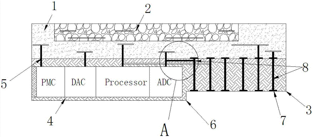
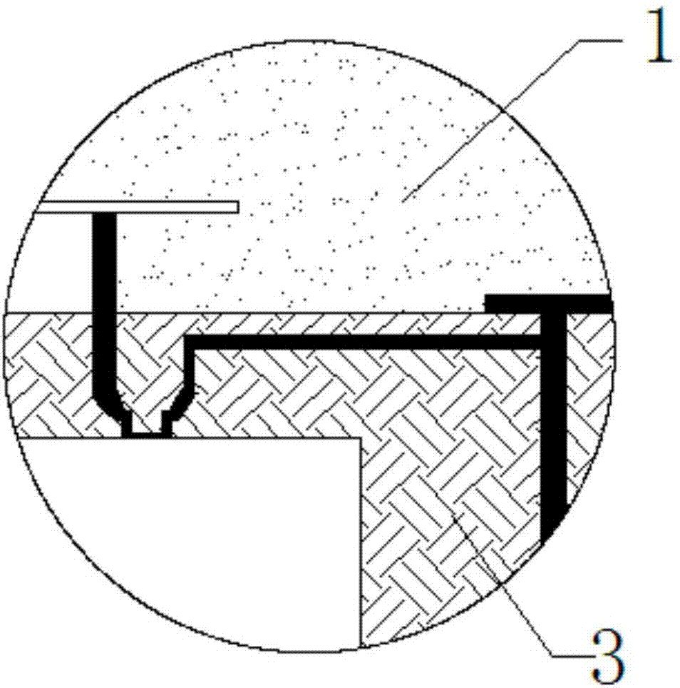
[0023] like figure 2 and image 3 As shown, an integrated system fingerprint chip packaging structure includes a substrate 1, a fingerprint chip 2, a plastic package 3 and a processing and control device 4, wherein the fingerprint chip 2 is arranged on the upper surface of the substrate 1, and the fingerprint chip 2 and the substrate 1 The circuit is electrically connected, the plastic package body 3 is plastic-sealed on the lower surface of the substrate 1, and the processing and control device 4 is completely wrapped inside it, so that the processing and control device 4 is located under the substrate 1, and the processing and control device 4 is connected to the sub...


PUM


Abstract

The invention discloses an integrated system fingerprint chip packaging structure and a fingerprint module. By taking fingerprint chip packaging and fingerprint module processing as the starting point, the fingerprint chip packaging is thinned, the fingerprint module processing structure is reduced, and the fingerprint structure is packaged systematically, wherein a fingerprint sensing region and a fingerprint substrate circuit are combined; control and processing devices are inversely placed below a substrate, and the substrate circuit and the control and processing devices are connected in a copper column manner; an EMC material is packaged reversely, and meanwhile, the connecting circuit is drawn to a windowing solder pad which is exposed below the fingerprint chip through an RDL way; and a mobile phone main board can be directly connected with the fingerprint chip through an elastic sheet way. By virtue of the integrated system fingerprint chip packaging structure, the fingerprint module can be ultra-thin and simple, and higher reliability and usability can be achieved.

Description

technical field [0001] The invention relates to the technical field of semiconductor packaging, in particular to an integrated system fingerprint chip packaging structure and an integrated system fingerprint module. Background technique [0002] The needs of the market are driving the transformation and development of technology, and these transformations and developments have greatly satisfied consumers' new needs and experience for electronic consumer goods such as mobile phones. Among them, the application of fingerprint recognition technology on mobile phones has improved the convenience and safety experience of consumers on mobile phones. Therefore, fingerprint recognition technology has quickly become the standard configuration of mobile phones. [0003] With the continuous development of high-performance mobile phones, it is an inevitable development trend to compress the space of fingerprint modules. Under the current trend, part of the fingerprint position is tran...

Claims


Application Information

Patent Timeline
Patent Type & Authority Applications(China)
IPC IPC(8): H01L23/31H01L23/498H01L25/065G06K9/00
CPCH01L23/49811H01L25/0655H01L23/3114G06V40/12
Inventor 王茂许杨柳高涛涛王林
Owner 昆山丘钛生物识别科技有限公司
Why Eureka
Try Eureka