Insulated gate power semiconductor device and method for manufacturing such a device
A technology of power semiconductors and insulated gates, which is applied in the field of power electronics to achieve the effect of improving device reliability and reducing risks
- Summary
- Abstract
- Description
- Claims
- Application Information
AI Technical Summary
Problems solved by technology
Method used
Image

Examples
Embodiment Construction
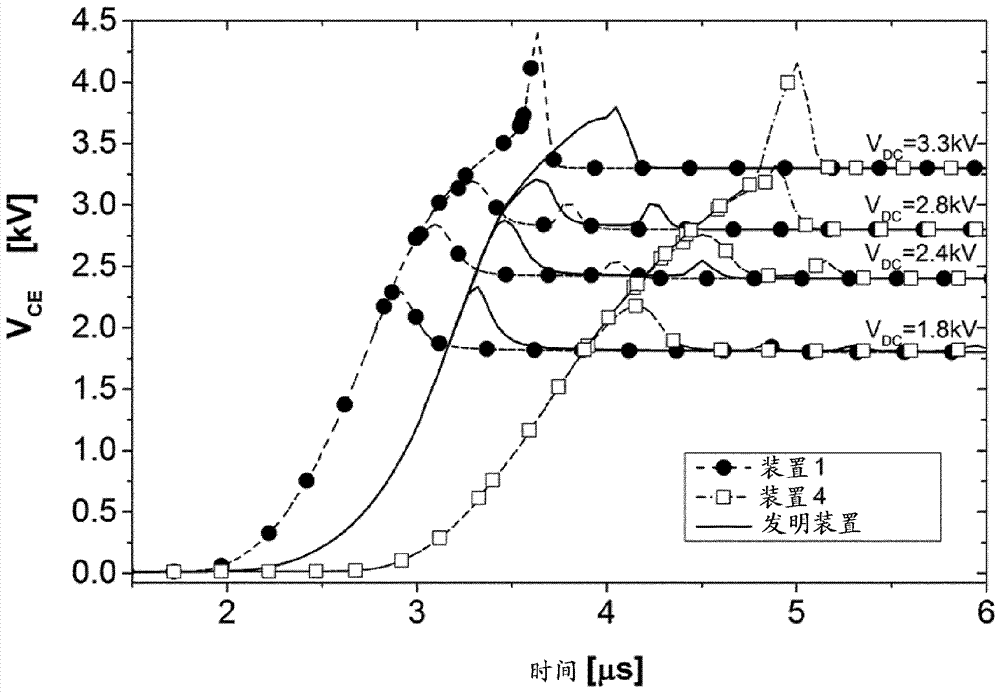
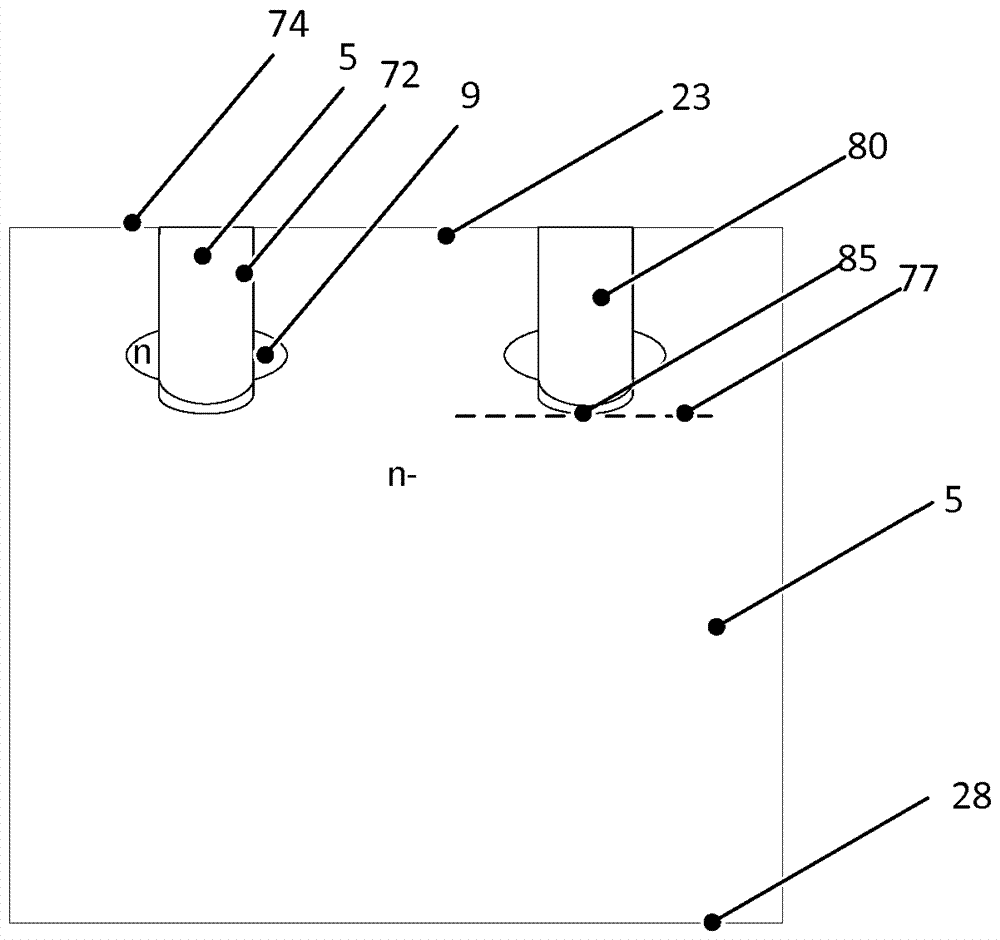
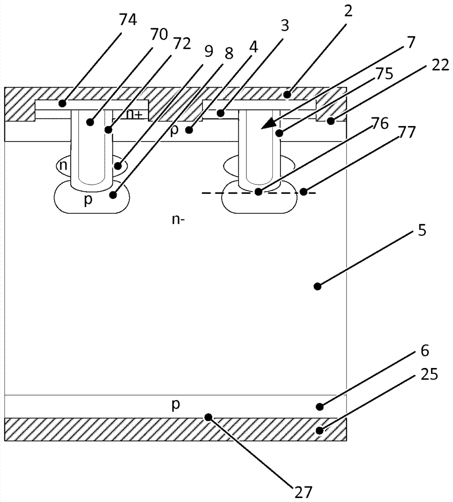
[0052] figure 2 , An inventive insulated gate power semiconductor device in the form of an insulated gate bipolar transistor 1 is shown, which includes an emitter electrode 2 on the emitter side 22 and a collector electrode 25 on the collector side 27, the collector side 27 is arranged opposite to the emitter side 22. The (n-) doped drift layer 5 is arranged between the emitter side 22 and the collector side 27. The p-doped base layer 4 is arranged between the drift layer 5 and the emitter side 22. The base layer 4 contacts the emitter electrode 2. At least one n-doped source layer 3 is arranged on the emitter side 22. The source layer 3 (which is separated from the drift layer 5 by the base layer 4) contacts the emitter electrode 2. The source layer 3 may be arranged such that the source layer 3 is arranged at both sides of each gate electrode 7.
[0053] The device includes: at least one trench gate electrode 7 having a conductive gate layer 70; and a first electrically in...
PUM
 Abstract
Description
Claims
Application Information
 - Generate Ideas
- Intellectual Property
- Life Sciences
- Materials
- Tech Scout
- Unparalleled Data Quality
- Higher Quality Content
- 60% Fewer Hallucinations
Browse by: Latest US Patents, China's latest patents, Technical Efficacy Thesaurus, Application Domain, Technology Topic, Popular Technical Reports.
© 2025 PatSnap. All rights reserved.Legal|Privacy policy|Modern Slavery Act Transparency Statement|Sitemap|About US| Contact US: help@patsnap.com