Method for checking and deleting dangline via in PCB design

An in-operation and object technology, applied in computing, special data processing applications, instruments, etc., can solve problems such as via holes increase design cost, PCB board inspection efficiency is low, and design quality is affected, so as to reduce design cost and improve design quality. , the effect of improving efficiency

Inactive Publication Date: 2017-10-17
ZHENGZHOU YUNHAI INFORMATION TECH CO LTD
View PDF7 Cites 7 Cited by
  • Summary
  • Abstract
  • Description
  • Claims
  • Application Information

AI Technical Summary

Problems solved by technology

[0005] The purpose of the present invention is to provide a method for checking and deleting dangling vias in PCB design, which is used to solve the problems of low inspection efficiency of existing PCB boards, excessive via holes increase design costs, and affect design quality.

Method used


Image

  • Method for checking and deleting dangline via in PCB design
  • Method for checking and deleting dangline via in PCB design
  • Method for checking and deleting dangline via in PCB design

Examples


Embodiment Construction

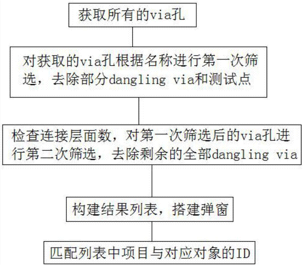
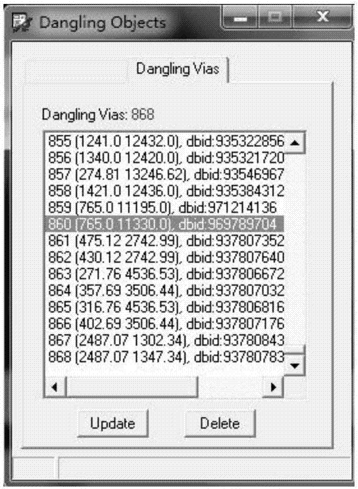
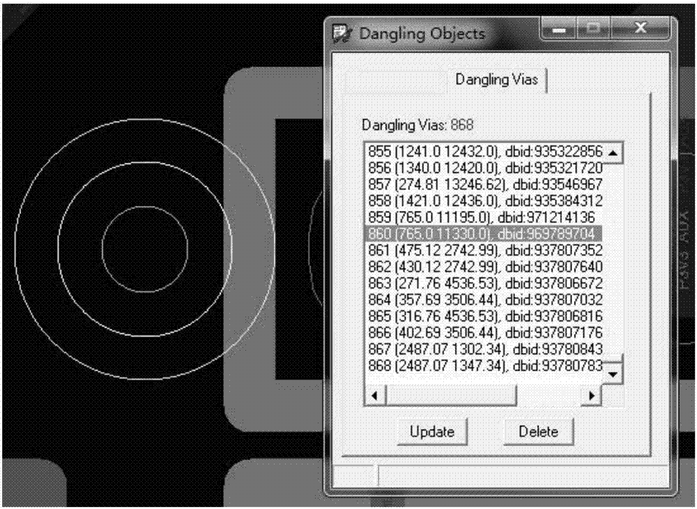
[0044] In order to clearly illustrate the technical features of the present solution, the present invention will be described in detail below through specific implementation methods and in conjunction with the accompanying drawings. The following disclosure provides many different embodiments or examples for implementing different structures of the present invention. To simplify the disclosure of the present invention, components and arrangements of specific examples are described below. Furthermore, the present invention may repeat reference numerals and / or letters in different instances. This repetition is for the purpose of simplicity and clarity and does not in itself indicate a relationship between the various embodiments and / or arrangements discussed. It should be noted that components illustrated in the figures are not necessarily drawn to scale. Descriptions of well-known components and processing techniques and processes are omitted herein to avoid unnecessarily lim...


PUM


Abstract

The invention discloses a method for checking and deleting dangling via in PCB design. The method specifically comprises the following steps of: 1) obtaining all the via holes; 2) carrying out first screening on the obtained via holes according to names and removing a part of the dangling via and test points; 3) checking the quantity of connection layers, carrying out second screening on the via holes after the first screening and removing all the residual dangling via; 4) constructing a result list and building a popup window; and 5) matching IDs of projects and corresponding objects in the list. According to the method, the dangling via can be rapidly checked and deleted, so that the complicated process of manual check in the design is simplified. The method is capable of avoiding missing, reducing the design cost and improving the design quality while improving the efficiency.

Description

technical field [0001] The invention relates to the technical field of post-checking of PCB boards, in particular to a method for checking and deleting dangling vias in PCB design. Background technique [0002] In the later stage of PCB design, engineers need to conduct a comprehensive and detailed inspection of the PCB board, which includes a wide range of aspects, including the inspection of dangling via. The via holes added in the early stage of design may be unused or used incorrectly. Such via holes are redundant objects and need to be checked out and deleted. [0003] What needs to be explained is that the unused or incorrect use mentioned here is limited by the size of the circuit board. The dense circuit board often uses via holes to achieve layer-changing routing. Sometimes the via holes punched during routing are not connected to the object at the end. This type is called unused. Sometimes the same via hole is only connected to one layer. This type is called incor...

Claims


Application Information

Patent Timeline
Patent Type & Authority Applications(China)
IPC IPC(8): G06F17/50
CPCG06F30/333G06F30/398
Inventor 张敏
Owner ZHENGZHOU YUNHAI INFORMATION TECH CO LTD
Why Eureka
Try Eureka