[0017] The application will be further described in detail below with reference to the drawings and embodiments. It is understandable that the specific embodiments described here are only used to explain the related application, but not to limit the application. In addition, it should be noted that, for ease of description, only parts related to the present application are shown in the drawings.
[0018] It should be noted that the embodiments in this application and the features in the embodiments can be combined with each other if there is no conflict. Hereinafter, the present application will be described in detail with reference to the drawings and in conjunction with embodiments.
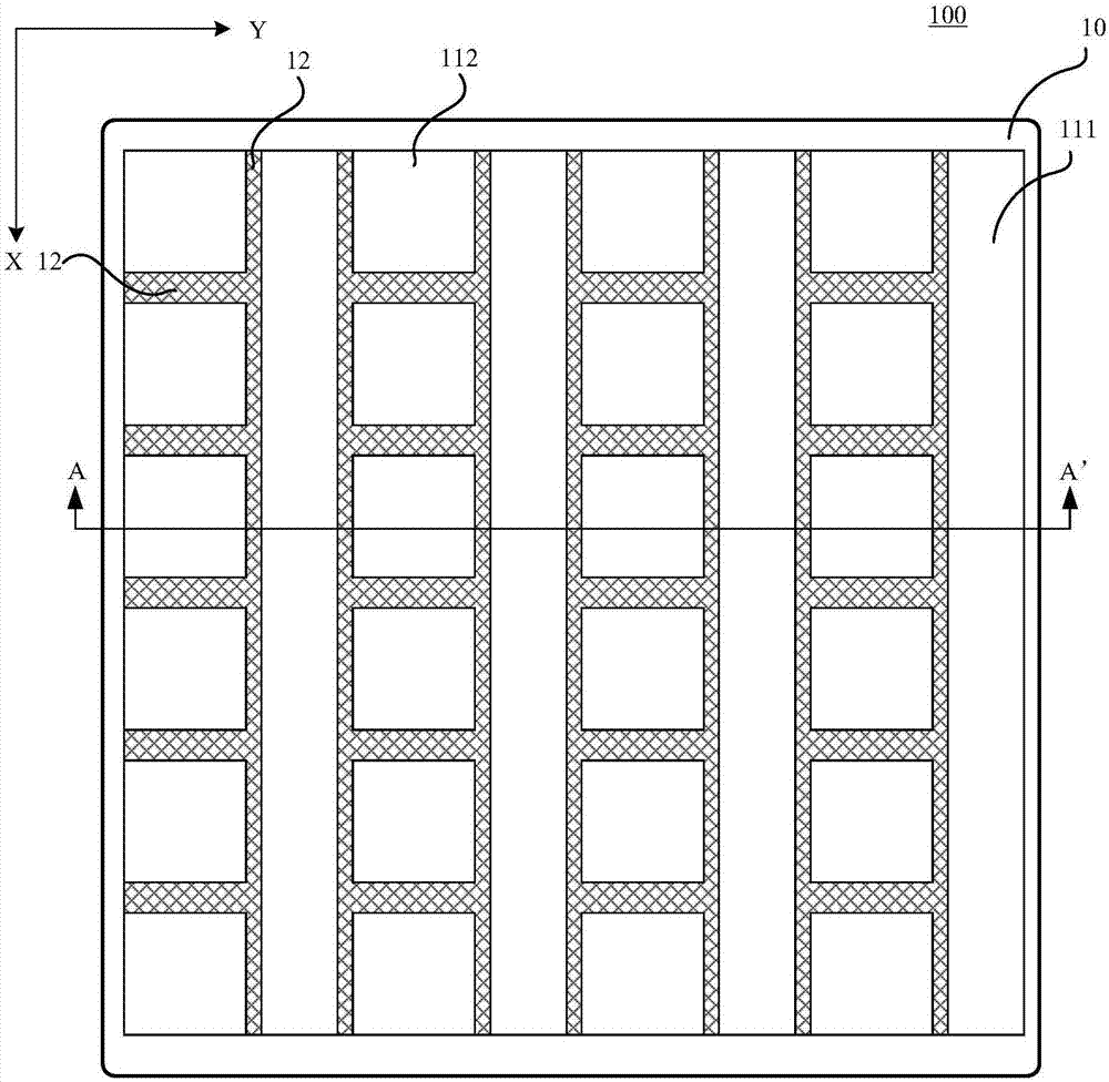
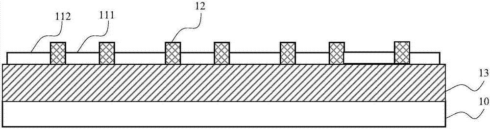
[0019] Please refer to figure 1 and figure 2 , figure 1 Shows a schematic structural diagram of the touch panel provided by the present application, figure 2 Shows along as figure 1 A cross-sectional view of AA' of the touch panel shown.
[0020] Such as figure 1 As shown, the touch panel 100 includes a base substrate 10, which may be a flexible base substrate, or a glass substrate, a quartz substrate, etc., and the base substrate 10 may provide support and protection for the touch panel.
[0021] A touch electrode layer is provided on the base substrate 10, and the touch electrode layer includes a plurality of first touch electrodes 111. Such as figure 1 As shown, the first touch electrodes 111 extend along the first direction X and are arranged along the second direction Y intersecting the first direction X. In this embodiment, the above-mentioned first touch electrode 111 may be rectangular.
[0022] The touch electrode layer further includes a plurality of second touch electrodes 112, and the second touch electrodes 112 are arranged in an array. The touch electrode 112 can be as figure 1 The rectangle shown can also be a triangle, a polygon, etc., which is not limited here. As long as it is satisfied that the second touch electrodes 112 are block-shaped and arranged in an array. The row direction of the second touch electrodes 112 is parallel to the first direction X, and the column direction of each second touch electrode 112 is parallel to the second direction Y. In some implementations, the first touch electrode may be a touch sensing electrode, and the second touch electrode may be a touch driving electrode.
[0023] In the embodiments of this application, such as figure 1 As shown, a plurality of second touch electrodes 112 are arranged between every two first touch electrodes 111, and the second touch electrodes 112 arranged between the first touch electrodes 111 are sequentially arranged along the first direction X cloth. In other words, the first touch electrodes 111 and the second touch electrodes 112 are alternately arranged. The principle of implementing the touch function in this embodiment is as follows: extending along the first direction X, the second touch electrodes in the same column arranged along the second direction Y constitute second touch electrode patterns intersecting the first touch electrodes. Any one of the first touch electrodes and at least one of the second touch electrodes has a facing area, thereby forming a touch capacitance. During touch, the second touch electrodes in the same column arranged along the second direction Y simultaneously receive the same touch drive signal, and the first touch electrodes extending across the second touch electrode pattern are used to receive touch sensing signal. When the user's finger touches any position on the display panel, the signal coupling between the second touch electrode and the first touch electrode near the touch point will change, so that the second touch electrode and the first touch electrode near the touch point will change. The capacitance of the touch capacitor formed between a touch electrode changes. The coordinates of the touch point in the second direction Y can be determined according to the first touch electrode 111, and the second touch electrode 112 can determine the coordinates of the touch point in the first direction X, so as to determine the touch of an object or finger on the touch panel 100. 控位。 Control position.
[0024] In this embodiment, since the first touch electrode 111 and the second touch electrode 112 are arranged on the same conductive layer, they can be arranged between the first touch electrode 111 and the second touch electrode 112 adjacent to it. There are insulating bumps 12, such as figure 2 Shown. The insulating protrusion 12 can block the first touch electrode 111 and the second touch electrode 112 from each other, so as to prevent the first touch electrode 111 and the second touch electrode 112 from being caused by external factors such as static electricity. One touch electrode 111 and the second touch electrode 112 are electrically connected to improve the touch accuracy of the touch panel 100.
[0025] The touch panel 100 may also be provided with an insulating layer 13, and the aforementioned touch electrode layer may be provided on the insulating layer 13. The protrusion 12 and the insulating layer 13 may be made of the same insulating material, or different insulating materials. Here, the insulating layer 13 can be used as a planarization layer between the touch electrode layer and the base substrate 10 to prevent the touch electrode layer from being directly disposed on the base substrate 10, resulting in the thickness of each touch electrode in the touch electrode layer. Uneven, thus affecting the touch effect.
[0026] It is worth noting here that the above-mentioned protrusions 12 may or may not be provided between the second touch electrodes 112 arranged along the first direction X.
[0027] Preferably, in order to prevent static electricity between the second touch electrodes 112 and prevent electrical connection between the second touch electrodes 112 due to static electricity or other factors between the second touch electrodes 112, A bump 12 is provided between the touch electrodes 112 arranged in the first direction X.
[0028] In this embodiment, the first touch electrode 111 and the second touch electrode 112 are arranged on the same layer of the touch panel 100, and at the same time, insulating protrusions are arranged between the first touch electrode 111 and the second touch electrode 112. The number of film layers of the touch panel 100 can be reduced, the manufacturing process of the touch panel 100 can be reduced, the yield rate of the touch panel 100 can be improved, and the first touch electrode 111 and the second touch electrode 112 can be isolated from each other. Improve the touch accuracy of the touch panel 100.
[0029] Preferably, the insulating material of the protrusion 12 can be an inorganic insulating material, and the inorganic insulating material can be, for example, silicon nitride, silicon oxide, or the like. By setting the material of the above-mentioned protrusion 12 as an inorganic insulating material, the first touch electrode 111 and the second touch electrode 112 can be better blocked from oxides such as water and oxygen, thereby improving the relationship between the first touch electrode 111 and the second touch electrode 112. The lifetime of the second touch electrode 112.
[0030] In this embodiment, the material of the above-mentioned first touch electrode 111 may be a transparent conductive material or a nano-metal material. The material of the second touch electrode 112 may also be a transparent conductive material, or a nano-metal material.
[0031] Since the bendability of nano-metal materials, especially nano-silver wire materials, is better than that of transparent conductive materials, in order to make the touch panel 100 more flexible, in some preferred implementation manners of this embodiment, the first One touch electrode 111 and the above-mentioned second touch electrode 112 are both formed of nano silver wire material.
[0032] In this embodiment, since the first touch electrode 111 and the second touch electrode 112 are arranged in the same layer, when the first touch electrode 111 and the second touch electrode 112 are both made of nano silver wire material, it is easy to produce The problem of silver ion migration is that silver ions are electrolyzed to produce silver ions under the action of an electric field and hydroxide ions. The migration of silver ions causes a bypass between the first touch electrode 111 and the second touch electrode 112, resulting in a short circuit between the first touch electrode 111 and the second touch electrode 112, thereby making the touch of the touch panel 100 The accuracy is reduced. By providing insulating protrusions between the first touch electrode 111 and the second touch electrode 112, the problem of silver ion migration can be reduced, and the touch accuracy of the touch panel 100 can be improved.
[0033] Please continue to refer Figure 3a-Figure 3d , Which shows a schematic diagram of the positional relationship between the first touch electrode and the second touch electrode provided in the present application.
[0034] In this embodiment, the first touch electrode 31 and the second touch electrode 32 are both disposed on the same conductive layer, and the first touch electrode 31 extends along the first direction X and along the second direction intersecting the first direction X Y settings. The second touch electrodes 32 are arranged in an array, the row direction of each second touch electrode 32 is parallel to the first direction X, and the column direction of the second touch electrodes 32 is parallel to the second direction Y. A plurality of second touch electrodes 32 are arranged between two adjacent first touch electrodes 31. The first touch electrodes 31 and the second touch electrodes 32 are insulated from each other by insulating protrusions 33.
[0035] In this embodiment, the first touch electrode 31 and the second touch electrode 32 may have overlapping regions.
[0036] Such as Figure 3a As shown, the first touch electrode 31 has a plurality of protrusions 311 that extend between two second touch electrodes 32 adjacent to the protrusion 311. The protrusion 311 of the first touch electrode 31 is disposed on one side of the first touch electrode 31. Wherein, the protrusion 311 of the first touch electrode 31 may be formed on the right side of the first touch electrode 31, or may be formed on the Figure 3a The left side of the first touch electrode 31 shown is not limited here. The above-mentioned implementation of the present application increases the intersecting and facing area between the first touch electrode and the second touch electrode, thereby increasing the mutual capacitance between the first touch electrode and the second touch electrode, which is beneficial to Improve the sensitivity of the touch panel.
[0037] The protrusions 311 of the first touch electrode 31 may also be formed on both sides of the first touch electrode 31 along the second reverse direction Y, and extend to both ends to the two second touch electrodes adjacent to the protrusion 311 Between 32, such as Figure 3b Shown.
[0038] Such as Figure 3c As shown, a plurality of recesses 321 may be formed on the second touch electrode 32, and the protrusions 311 of the first touch electrode 31 may extend to the recesses 321 of the second touch electrode 32. In this way, an overlapping area can also be formed between the first touch electrode 31 and the second touch electrode 32. Same as Figure 3c The second touch electrode 32 shown only illustrates the case where the protrusion 311 is disposed on one side, and the present application is not limited to this. In some other application scenarios, the protrusion 311 may also be disposed on the second touch electrode 32. The first touch electrodes on the two sides adjacent to the second touch electrodes 32 are provided with recesses 321.
[0039] The first touch electrode 31 may also be comb-shaped. Similarly, the second touch electrode 32 may also be comb-shaped, such as Figure 3d Shown. The comb teeth of the first touch electrode 31 and the comb teeth of the second touch electrode 32 adjacent thereto are alternately arranged. One of the first touch electrodes 31 and the plurality of second touch electrodes 32 are alternately arranged. In this way, the first touch electrode 31 and the second touch electrode 32 also have an overlapping portion. Further increase the intersecting facing area between the first touch electrode and the second touch electrode, thereby increasing the mutual capacitance between the first touch electrode and the second touch electrode, which is beneficial to improve the sensitivity of the touch panel .
[0040] It’s worth noting here that although this application provides Figure 3a-Figure 3d The arrangement between the first touch electrode 31 and the second touch electrode 32 is shown, but the present application is not limited to the above pattern, as long as the first touch electrode extends along the first direction X and along the second direction Y It is provided that the second touch electrodes are arranged in an array, and the overlapping areas between the first touch electrodes and the second touch electrodes adjacent thereto fall within the protection scope of the present application.
[0041] In this embodiment, by providing a staggered portion between the first touch electrode 31 and the second touch electrode 32, the mutual capacitance between the first touch electrode 31 and the second touch electrode 32 can be increased, so that the mutual capacitance between the first touch electrode 31 and the second touch electrode 32 can be increased. Accurately determine the position of the touch object or finger on the touch panel, thereby improving the sensitivity of the touch panel.
[0042] Continue to refer Figure 4 , Which shows a schematic structural diagram of another touch panel provided by the present application.
[0043] Such as Figure 4 As shown, the touch panel 400 includes a base substrate 40, a touch electrode layer disposed on the base substrate 40, and the touch electrode layer includes a second direction row extending along a first direction X and intersecting the first direction X The first touch electrodes 411 and the second touch electrodes 412 are arranged in an array.
[0044] In this embodiment, the touch panel 400 further includes a touch signal line 42 electrically connected to the second touch electrode 412, the touch panel 400 is further provided with an integrated circuit 43, and the touch signal line 42 connects the second touch electrode 412 Connect to the integrated circuit 43. During the touch, the integrated circuit 43 provides a touch drive signal to the second touch electrode 412 through the touch signal line 42, and the first touch electrode 411 outputs a touch detection signal. When a finger touches the touch panel 400, the first touch electrode 411 and the second touch electrode 412 are coupled, thereby changing the capacitance between the first touch electrode 411 and the second touch electrode 412. According to the received detection signal output by each first touch electrode 411, the variable of the capacitance is determined, and then the touch position is determined.
[0045] In the above-mentioned embodiments of the present application, by arranging the first touch electrode and the second touch electrode on the same touch electrode layer, the number of film layers of the touch panel can be reduced, the manufacturing process complexity of the touch panel is reduced, and the touch panel is improved The yield rate of the flexible touch panel can also improve the bending resistance of the panel. At the same time, an insulating protrusion is provided between the first touch electrode and the second touch electrode, which can prevent short circuit between the first touch electrode and the second touch electrode due to problems such as static electricity and ion migration, and improve touch control. The touch accuracy of the panel.
[0046] It should be noted that the touch signal line 42 and the second touch electrode 412 may be disposed on the same conductor layer, that is, on the touch electrode layer 41, or may be disposed on a different conductor layer from the second touch electrode 412. When the touch signal line 42 and the second touch electrode 412 are disposed on different conductive layers, the touch signal line 42 can be connected to the second touch electrode 412 through a via hole.
[0047] In some implementations, the touch signal line 42 and the second touch electrode 412 are arranged on the same conductive layer, and the arrangement is as follows Figure 4 Shown. By arranging the touch signal line 42 and the second touch electrode 412 on the same conductive layer, the number of film layers of the touch panel 400 can be further reduced, the manufacturing process of the touch panel 400 can be reduced, and the yield rate of the touch panel 400 can be improved. . In addition, for a flexible touch panel, the bending resistance of the panel can also be improved.
[0048] In this embodiment, the touch panel 400 further includes a light emitting diode array 44 disposed between the base substrate 40 and the touch electrode layer 41, such as Figure 5 As shown, Figure 5 A cross-sectional view of the touch panel 400 along BB' is shown. The aforementioned light emitting diode array 44 may include a plurality of organic light emitting diodes arranged in an array. The organic light emitting diode may include a stacked first electrode, an organic light emitting layer, and a second electrode, wherein the organic light emitting layer is disposed between the first electrode and the second electrode. The touch panel 400 further includes an encapsulation layer 45 covering the aforementioned light emitting diode array 44. The encapsulation layer may be formed of at least one inorganic layer and at least one organic layer. Among them, the light-emitting diode array 44 can be an inorganic layer. Since the inorganic layer has a strong ability to block water and oxygen, it can be determined that the light-emitting diode array 44 is not affected by moisture and oxygen, thereby improving the performance of the light-emitting diode 44. life.
[0049] In this embodiment, the touch panel 400 further includes an insulating layer 46 disposed on a side of the packaging layer 45 away from the base substrate 40. The insulating layer 46 is provided with a plurality of first grooves 461 and second grooves 462 insulated from each other. The groove provided on the insulating layer 46 separates the touch electrode layer 41 into the first touch electrode 411 and the second touch electrode 412. In other words, the first touch electrode 411 is disposed in the first groove 461, and the second touch electrode 412 is disposed in the second groove 462. Here, the convex portions on both sides of the first groove 461 and the second groove 462 separate the first touch electrode 411 from the second touch electrode 412. Here, the material of the insulating layer 45 may be an inorganic layer. In this way, the thin film encapsulation layer can be further isolated from water and oxygen, and the touch accuracy of the touch panel can be improved.
[0050] In some implementation manners of the foregoing embodiments of the present application, the foregoing touch panel may be a flexible touch display panel, and the flexible touch display panel adopts a film encapsulation method to seal the organic light-emitting layer to achieve the effect of blocking water and oxygen. In the embodiment of the present application, the first touch electrode and the second touch electrode are arranged in the groove of the thin film packaging layer away from the base substrate, and the first touch electrode and the second touch electrode are arranged on the same touch electrode The layer can reduce the number of film layers of the touch panel, reduce the complexity of the manufacturing process of the touch panel, increase the yield of the touch panel, and also improve the bending resistance of the panel. In addition, an insulating protrusion is provided between the first touch electrode and the second touch electrode, which can prevent short-circuit between the first touch electrode and the second touch electrode due to problems such as static electricity and ion migration, thereby improving touch control. The touch accuracy of the panel.
[0051] It should be noted that the touch display panel of the above embodiment of the present application may be a flexible or rigid OLED touch display panel, but those skilled in the art should understand that the touch display panel of the embodiment of the present application is also applicable to other Any possible display technology form, such as micro LED display (micro LED), quantum dot display (Quantum Dot Light Emitting Diodes, QLED), electronic paper, etc., and there is no limitation on the flexibility or rigidity of the panel, and the specific options can be selected according to requirements And settings.
[0052] Please continue to refer Image 6 , Which shows the process 600 of the manufacturing method of the touch panel provided by the present application.
[0053] Step 601: Provide a base substrate.
[0054] In this embodiment, the touch panel can be a flexible panel or a rigid panel. The material of the above-mentioned base substrate may be glass, quartz or the like. When the touch panel is a flexible substrate, a thin film packaging layer can be formed on the base substrate, and after the thin film packaging layer is formed, the thin film packaging layer is peeled off from the base substrate.
[0055] Step 602, deposit a touch electrode layer on the base substrate.
[0056] In this embodiment, a touch electrode layer may be deposited on the base substrate, and the touch electrode layer includes a first touch electrode and a second touch electrode. The first touch electrodes extend in a first direction and are arranged in a second direction intersecting the first direction, and the second touch electrodes are arranged in an array. The row direction of the second touch electrodes is parallel to the first direction, the column direction of the second touch electrodes is parallel to the second direction, and a plurality of second touch electrodes are arranged between every two adjacent first touch electrodes . In some implementations, the first touch electrode may be a touch sensing electrode of a touch panel, and the second touch electrode may be a touch driving electrode of the touch panel.
[0057] Step 603, forming an insulating protrusion between the first touch electrode and the adjacent second touch electrode.
[0058] In this embodiment, in order to insulate the first touch electrode and the second touch electrode from each other and prevent the first touch electrode and the second touch electrode from being electrically connected to reduce the touch accuracy of the touch panel, An insulating protrusion is formed between the first touch electrode and the second touch electrode adjacent thereto. Compared with organic materials, inorganic materials have better barrier capabilities and can block water and oxygen in the air. Therefore, inorganic materials can be used to form the above-mentioned insulating protrusions.
[0059] The touch panel produced by this embodiment can refer to figure 1.
[0060] In some optional implementations of this embodiment, depositing the touch electrode layer on the base substrate includes: depositing an insulating layer on the base substrate; etching the insulating layer to form a plurality of mutually insulated grooves; In printing technology, patterned first touch electrodes and second touch electrodes are formed in a groove, wherein the first touch electrode and the second touch electrode are formed in the groove; the material used for inkjet printing is nano Silver wire slurry.
[0061] In some optional implementations of this embodiment, depositing the touch electrode layer on the base substrate includes: depositing an insulating layer on the base substrate; etching the insulating layer to form a plurality of grooves insulated from each other; A conductive layer is deposited on the layer, and the conductive layer is etched to form a first touch electrode and a second touch electrode, wherein the first touch electrode and the second touch electrode are formed in the groove.
[0062] In some optional implementations of this embodiment, the manufacturing method of the touch panel further includes a step of forming a touch signal line and electrically connecting the touch signal line with the second touch electrode. This step is formed on the substrate Before depositing the touch electrode layer on the substrate, this step includes: depositing a metal conductor layer on the base substrate, and the metal conductor layer may be used to form a plurality of touch signal lines. An insulating layer is deposited on the first conductive layer, and the insulating layer is etched to form a via hole for connecting the touch signal line and the touch electrode.
[0063] This embodiment provides a touch device, such as Figure 7 Shown. The present embodiment relates to that the touch display device 700 can be used in various devices such as smart phones, tablet terminals, mobile phone terminals, notebook-type personal computers, and game equipment. Specifically, the touch device 700 includes the touch panel mentioned in any of the foregoing embodiments.
[0064] In the touch panel, the manufacturing method thereof, and the touch device provided by the embodiments of the present application, the number of film layers of the touch panel can be reduced by arranging the first touch electrode and the second touch electrode on the same touch electrode layer. Reduce the complexity of the manufacturing process of the touch panel, and improve the yield of the touch panel. At the same time, an insulating protrusion is provided between the first touch electrode and the second touch electrode, which can prevent short circuit between the first touch electrode and the second touch electrode due to problems such as static electricity and ion migration, and improve touch control. The touch accuracy of the panel.
[0065] Those skilled in the art should understand that the scope of the technical solutions involved in this application is not limited to the technical solutions formed by the specific combination of the above technical features, and should also cover the technical solutions described above without departing from the concept of the technical solutions. Other technical solutions formed by any combination of technical features or equivalent features. For example, the above-mentioned features and the technical features disclosed in this application (but not limited to) with similar functions are mutually replaced to form a technical solution.