Organic light emitting diode (OLED) display panel and OLED spliced display screen with same

A display panel and substrate technology, applied in the direction of instruments, electrical components, electrical solid devices, etc., can solve problems such as inability to achieve seamless splicing, discontinuous screen images, and affecting viewing effects, so as to reduce non-luminous areas and optimize Stitching effect, the effect of small seams

Inactive Publication Date: 2012-10-24
GUANGDONG VTRON TECH CO LTD
View PDF4 Cites 33 Cited by
  • Summary
  • Abstract
  • Description
  • Claims
  • Application Information

AI Technical Summary

Problems solved by technology

like image 3 As shown, when the OLED panels are spliced ​​into a large screen, splicing gaps will be left, and the non-luminous frame area - the packaging plastic frame 2 and the external circuit binding area 3 cannot display images, resulting in discontinuous screen images and affecting the viewing effect
Many panel manufacturers are committed to improving the manufacturing process, but only relying on the improvement of the manufacturing process can only narrow the seam as much as possible, but cannot achieve the effect of seamless splicing

Method used


Image

  • Organic light emitting diode (OLED) display panel and OLED spliced display screen with same
  • Organic light emitting diode (OLED) display panel and OLED spliced display screen with same
  • Organic light emitting diode (OLED) display panel and OLED spliced display screen with same

Examples


Embodiment 1

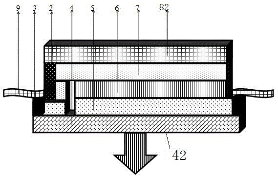
[0034] Such as Figure 4 As shown, an OLED display panel includes a substrate 4, an OLED module, and an encapsulation layer. The OLED module is arranged on the substrate 4, and the encapsulation layer is arranged on the periphery and the front of the OLED module; wherein the OLED module includes an anode layer 5, a cathode layer 7 and a The organic layer 6 between the anode layer 5 and the cathode layer 7 , the anode layer 5 is disposed on the first layer on the substrate 4 , and the encapsulation layer is disposed on the front of the cathode layer 7 . The light-emitting surface of the display panel is located on the back surface 42 of the substrate. There are perforations in the structure formed by the OLED module and the encapsulation layer. The through-holes are respectively filled with conductive substances to form cathodes and anodes. pixel, each light-emitting pixel in the OLED module is provided with a perforation 11, wherein the perforation 11 passes through the organi...

Embodiment 2

[0038] Such as Figure 5 As shown, the structure of this embodiment is roughly the same as that of Embodiment 1, except that the OLED module in the OLED display panel adopts an inverted structure. The cathode layer 7 of the OLED module is arranged on the first layer on the substrate 4 , and the encapsulation layer is arranged on the front of the anode layer 5 . The light-emitting surface of the display panel is located on the back of the substrate. There are perforations in the structure formed by the OLED module and the encapsulation layer. The through-holes are filled with conductive substances to form the cathode and anode respectively. The structure of the perforations is refined to each light-emitting pixel in the OLED module. , each light-emitting pixel in the OLED module is provided with a perforation 11, wherein the perforation 11 passes through the organic layer 6 and the anode layer 5, and the encapsulation layer is provided with two perforations 10 corresponding to ...

Embodiment 3

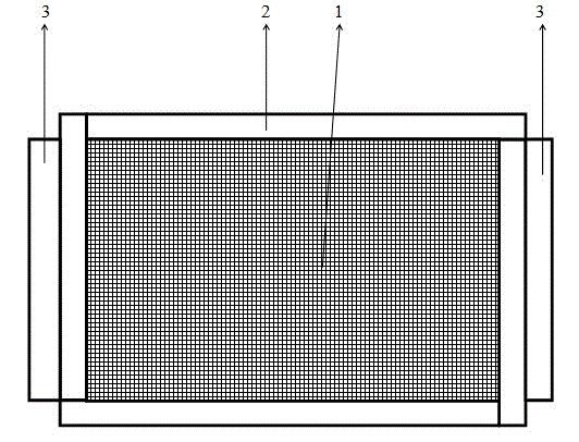
[0041] Such as Figure 6 As shown, the structure of this embodiment is roughly the same as that of Embodiment 1, the difference is that the encapsulation layer in the OLED display panel is encapsulated by the traditional encapsulation back cover 82, wherein the encapsulation layer includes the encapsulation back cover 82 and the encapsulation plastic frame 2 The encapsulation back cover 82 adopts a transparent glass flexible encapsulation panel and is arranged on the front of the OLED module. The encapsulation back cover 82 reserves mounting holes as perforations 10, and the anode and the cathode respectively extend outward through the mounting holes on the encapsulation back cover 82 and are exposed on the encapsulation back cover. 82, the anode and cathode are sealed between the mounting holes. The encapsulating plastic frame 2 is arranged around the OLED module, one end of which is in sealing contact with the encapsulating back cover 82 , and the other end is in sealing con...


PUM


Abstract

The invention relates to the organic light emitting diode display technology, in particular to an organic light emitting diode (OLED) display panel and an OLED spliced display screen with the same. The OLED display panel comprises a base plate, wherein the base plate is provided with an OLED module; the periphery and the upper part of the OLED module are provided with packaging layers; a structure formed by the OLED module and the back of the luminous surface of the display panel is provided with perforations from which a cathode and an anode are respectively introduced to the back of the luminous direction of the display panel; the positions for introducing the cathode and the anode on the back of the luminous surface of the display panel are respectively provided with conducting film layers which are not mutually connected; and a bonding area of an external-connection circuit is introduced out of the conducting film layers. According to the OLED display panel disclosed by the invention, the bonding area of the external-connection circuit is transferred to the back of the luminous surface of the device from the periphery of the OLED module edge so as to greatly reduce the non-luminous area of the device, and the OLED spliced display screen formed by splicing the OLED display panel is provided with a smaller abutted seam so as to optimize the splicing effect of the OLED spliced display screen.

Description

technical field [0001] The invention relates to an organic light emitting diode (OLED) display technology, in particular to an OLED display panel and an OLED splicing display screen with the display panel. Background technique [0002] OLED has the advantages of self-luminescence, all-solid-state, ultra-thin, no viewing angle limitation, fast response, wide operating temperature, easy to realize flexible display and 3D display, etc., and is considered to be one of the most promising new FPD technologies. At present, the largest OLED screen that can be trial-produced is below 55 inches, and the OLED screens that are commercially put on the market are limited to 5-10 inches, and the size is small. Expensive raw materials. Therefore, how to use existing size OLED panels to further assemble and splice into a large-screen video wall to meet the requirements of large-screen display has become an important issue in this technical field. [0003] According to the requirements of t...

Claims


Application Information

Patent Timeline
Patent Type & Authority Applications(China)
IPC IPC(8): H01L27/32G09F9/33
Inventor 彭晓林匡友元孙婷黄永峰
Owner GUANGDONG VTRON TECH CO LTD
Why Eureka
Try Eureka