OLED device and manufacturing method thereof

A manufacturing method and device technology, applied in semiconductor/solid-state device manufacturing, organic light-emitting device manufacturing/processing, electric solid-state devices, etc., can solve the problems of low adjustment flexibility and single adjustment method, and achieve the effect of improving adjustment flexibility

Active Publication Date: 2017-10-20
BOE TECH GRP CO LTD
View PDF6 Cites 26 Cited by
  • Summary
  • Abstract
  • Description
  • Claims
  • Application Information

AI Technical Summary

Problems solved by technology

[0006] However, at present, the adjustment method of the total optical path difference can only be adjusted by adjusting the thickness of the above-mentioned organic film layer, and the adjustment method is single, so the adjustment flexibility is low

Method used


Image

  • OLED device and manufacturing method thereof
  • OLED device and manufacturing method thereof

Examples


Embodiment Construction

[0038] In order to enable those skilled in the art to better understand the technical solution of the present invention, the OLED device provided by the present invention and its manufacturing method will be described in detail below with reference to the accompanying drawings.

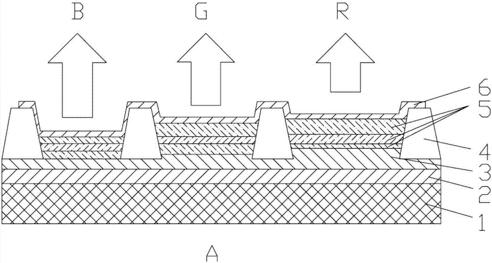
[0039] figure 1 It is a cross-sectional view of the OLED device provided by the first embodiment of the present invention. see figure 1 , the OLED device provided by the present invention includes a substrate 1 and a plurality of pixel units located on the substrate 1, figure 1 An arbitrary pixel unit A is shown. Each pixel unit A includes a first electrode layer 2 , an organic layer 5 and a microcavity effect adjustment structure 3 . The first electrode layer 2 is disposed on the substrate 1 and is an opaque reflective anode. The microcavity effect adjustment structure 3 is arranged on the first electrode layer 2; the organic layer 5 is arranged on the microcavity effect adjustment structure 3; th...


PUM

PropertyMeasurementUnit
thicknessaaaaaaaaaa
thicknessaaaaaaaaaa
electron work functionaaaaaaaaaa

Abstract

The invention provides an OLED device and a manufacturing method thereof. The OLED device includes a substrate and a plurality of pixel units on the substrate. Each of the pixel units includes a first electrode layer, an organic layer, and a second electrode layer. The OLED device is characterized by comprising a micro-cavity effect adjusting structure including at least one transparent oxide layer disposed between the first electrode layer and the organic layer. The OLED device and the manufacturing method thereof add a way of adjusting the total optical path difference in optical design so as to improve adjustment flexibility.

Description

technical field [0001] The invention relates to the field of display technology, in particular to an OLED device and a manufacturing method thereof. Background technique [0002] Large-size OLED display technology has become a favored technology for large-size high-end TV applications because of its strong dark-state expressiveness and high contrast ratio. However, due to the limitations of OLED material costs and process yields, its market share is not high. Although the large-size OLED display processed by the solution method is expected to greatly reduce the manufacturing cost by depositing OLED ink materials through inkjet printing technology, but the current bottom emission printed OLED display devices have low aperture ratio, poor luminous efficiency, and small color reproduction range. , short lifespan and other limitations, so top-emitting OLED display devices that can technically solve these limitations have attracted a lot of research and development interest, and ...

Claims


Application Information

Patent Timeline
Patent Type & Authority Applications(China)
IPC IPC(8): H01L51/50H01L51/52H01L51/56
CPCH10K30/865H10K50/80H10K50/00H10K2102/301H10K71/00
Inventor 黄维
Owner BOE TECH GRP CO LTD
Why Eureka
Try Eureka