
Heat dissipation structure of semiconductor device and semiconductor device

A heat dissipation structure, semiconductor technology, applied in the direction of semiconductor devices, semiconductor/solid-state device parts, electric solid-state devices, etc., can solve the problems of low output power of semiconductor devices, poor cooling effect of semiconductor devices, etc., to improve service life and ensure output The effect of power

Active Publication Date: 2017-11-03
DYNAX SEMICON
View PDF7 Cites 5 Cited by
  • Summary
  • Abstract
  • Description
  • Claims
  • Application Information

AI Technical Summary

Problems solved by technology

[0004] In view of this, an embodiment of the present invention provides a heat dissipation structure of a semiconductor device and a semiconductor device to solve the technical problems of poor cooling effect of the semiconductor device and low output power of the semiconductor device in the prior art

Method used


Image

  • Heat dissipation structure of semiconductor device and semiconductor device
  • Heat dissipation structure of semiconductor device and semiconductor device
  • Heat dissipation structure of semiconductor device and semiconductor device

Examples


Embodiment Construction

[0033] In order to make the purpose, technical solution and advantages of the present invention clearer, the technical solution of the present invention will be fully described below through specific implementation in combination with the drawings in the embodiments of the present invention. Apparently, the described embodiments are some embodiments of the present invention, rather than all embodiments. Based on the embodiments of the present invention, all other embodiments obtained by persons of ordinary skill in the art without making creative efforts, All fall within the protection scope of the present invention.

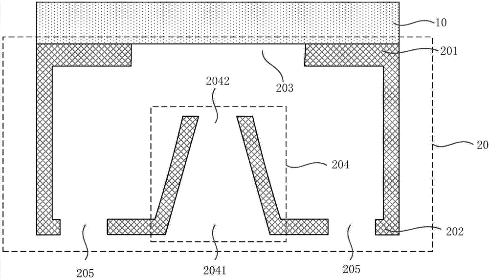
[0034] figure 1 It is a structural schematic diagram of a heat dissipation structure of a semiconductor device provided by an embodiment of the present invention, such as figure 1 As shown, the heat dissipation structure of the semiconductor device provided by the embodiment of the present invention may include:

[0035] The upper surface 201 of the heat dissi...


PUM


Abstract

The embodiment of the invention discloses a heat dissipation structure of a semiconductor device, and a semiconductor device, and relates to the technical field of semiconductors. The heat dissipation structure of the semiconductor comprises an upper surface close to one side of the semiconductor device, a lower surface far away from one side of the semiconductor device, and at least one heat dissipation channel, wherein a heat dissipation window is formed in the upper surface; and the at least one heat dissipation channel comprises an inlet and an outlet, the inlet is arranged to be opposite to the heat dissipation window, the inlet comprises a first cross section and a second cross section, and the opening area of the first cross section is more than that of the second cross section. According to the technical scheme of the structure provided by the invention, the inlet of the heat dissipation channel is corresponding to the first heat dissipation window, the area of the first cross section of the inlet is more than that of the second cross section, the condition that a heat conduction medium flowing in via the inlet has a high flow speed at the second cross section is ensured, fat dissipation of heat of the semiconductor device is ensured, and normal output power of the semiconductor device is also ensured.

Description

technical field [0001] The embodiments of the present invention relate to the technical field of semiconductors, and in particular to a heat dissipation structure of a semiconductor device and the semiconductor device. Background technique [0002] With the maturity of GaN device technology, the advantages of high power density of GaN devices are more clearly displayed, and the industry gradually begins to mass-produce GaN devices. However, as the integration level of integrated circuits increases, higher requirements are placed on the heat dissipation of GaN devices. According to measurements, the heat distribution of GaN devices is mainly concentrated near the Schottky junction of the device, which can continuously generate heat, and when the heat cannot be effectively dissipated, the temperature of the Schottky junction will increase, thereby degrade the power output and RF performance of the device. [0003] Traditional thermal management technologies are represented b...

Claims


Application Information

Patent Timeline
Patent Type & Authority Applications(China)
IPC IPC(8): H01L23/46
CPCH01L23/46H01L23/473H01L23/467H01L23/367H01L23/3732H01L23/3738H01L23/42
Inventor 吴传佳裴轶
Owner DYNAX SEMICON
Learn More