Micro LED chip, manufacturing method thereof, and Micro LED array substrate

A manufacturing method and chip technology, applied in the field of optoelectronics, can solve the problems of decreased luminous efficiency, loss of the light-emitting area of ​​MicroLED chips, etc., and achieve the effects of saving occupied area, improving reliability and manufacturing cost, and avoiding shading

Active Publication Date: 2017-11-07
XIAMEN CHANGELIGHT CO LTD
View PDF4 Cites 15 Cited by
  • Summary
  • Abstract
  • Description
  • Claims
  • Application Information

AI Technical Summary

Problems solved by technology

[0005] In view of this, the present invention provides a Micro LED chip and its manufacturing method to solve the problems of serious loss of light-emitting area and decreased luminous efficiency of Micro LED chips in the prior art

Method used


Image

  • Micro LED chip, manufacturing method thereof, and Micro LED array substrate
  • Micro LED chip, manufacturing method thereof, and Micro LED array substrate
  • Micro LED chip, manufacturing method thereof, and Micro LED array substrate

Examples


Embodiment Construction

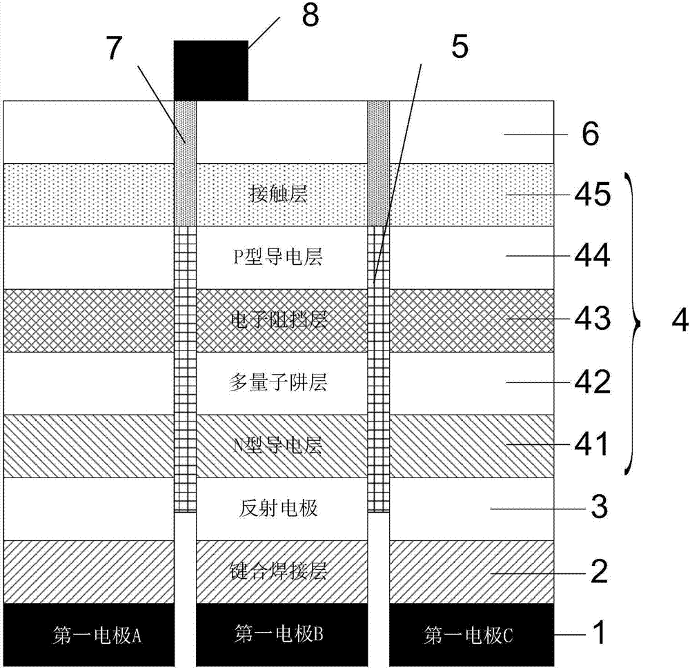
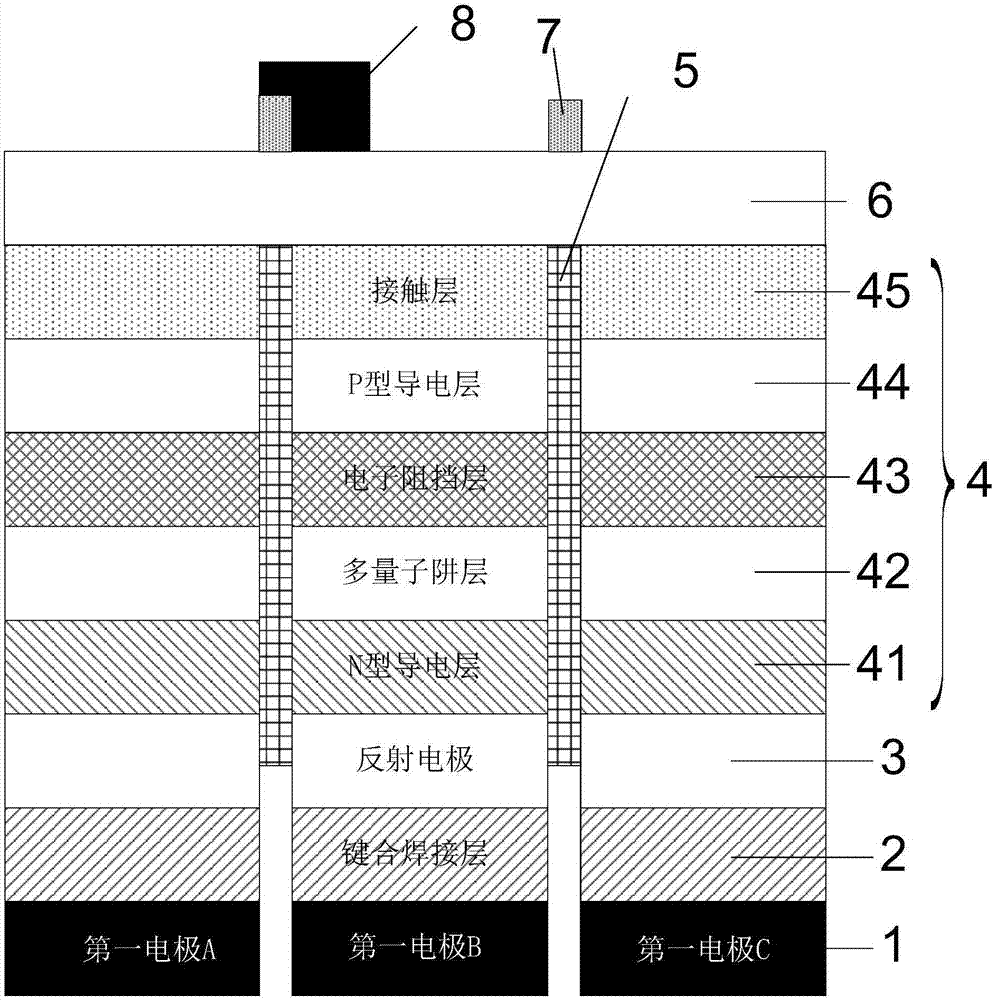
[0063] As mentioned in the background technology section, the Micro LED in the prior art suffers from serious loss of light-emitting area, and the luminous efficiency drops significantly.

[0064] The inventors found that the reason for the above phenomenon is that the same-side electrodes are used in the production process of the Micro LED chip, and the same-side electrodes need to be made in the LED chip of each unit, and the same-side electrodes need to be etched through the active area, while the area of ​​Micro LED chips is small and the number of chips is large, the real sun will occupy a large chip area, resulting in a serious loss of the entire Micro LED light-emitting area, which in turn leads to a significant drop in luminous efficiency.

[0065] Based on this, the present invention provides a Micro LED chip, including:

[0066] a plurality of first electrodes arranged in an array and insulated from each other;

[0067] reflective electrodes electrically connected t...


PUM


Abstract

The application provides a Micro LED chip, a manufacturing method thereof, and a Micro LED array substrate. The Micro LED chip uses a vertical structure. A first electrode and a second electrode are manufactured on different sides respectively. By arranging an electrode net with a grid structure on an isolation layer, multiple Micro LED sub-chips can emit light independently as long as only one second electrode is electrically connected with the electrode net and there is no need to provide a second electrode for each Micro LED sub-chip for light emitting control. The electrode net is arranged on the isolation layer, and the position of the electrode net is opposite to the position of the isolation layer to avoid the blocking of the effective light-emitting area by the electrode net, thereby greatly reducing the light-blocking area of the electrode. Compared with the prior art, the Micro LED chip increases light-emitting area and improves light-emitting efficiency.

Description

technical field [0001] The present invention relates to the field of optoelectronic technology, in particular to a Micro LED chip, a manufacturing method thereof, and a Micro LED array substrate. Background technique [0002] Micro LED Display (Micro LED Display) is a new generation of display technology. The structure is a miniaturized LED array, that is, the LED structure design is thinned, miniaturized and arrayed, so that its volume is about the size of the current mainstream LED. Each pixel can be addressed and driven to emit light independently, reducing the distance between pixels from the original millimeter level to the micron level. [0003] Inheriting the characteristics of LED, the advantages of Micro LED include low power consumption, high brightness, ultra-high resolution and color saturation, fast response, super power saving, long life, high efficiency, etc., and its power consumption is about LCD 10%, 50% of OLED. Compared with OLED, which is also a self-l...

Claims


Application Information

Patent Timeline
Patent Type & Authority Applications(China)
IPC IPC(8): H01L33/00H01L33/06H01L33/10H01L33/38
CPCH01L33/005H01L33/0075H01L33/06H01L33/10H01L33/38
Inventor 林志伟陈凯轩李俊贤卓祥景汪洋
Owner XIAMEN CHANGELIGHT CO LTD
Why Eureka
Try Eureka