Microfluidic MEMS chip packaging method

A technology of chip packaging and microfluidic control, applied in the direction of microstructure devices, manufacturing microstructure devices, processing microstructure devices, etc., can solve the problems of unguaranteed quality, long production cycle, high cost, etc., to shorten the production cycle and improve the quality of finished products The effect of increasing the efficiency and improving the bonding accuracy

Inactive Publication Date: 2017-11-17
镇江华瑞芯片科技有限公司
View PDF7 Cites 6 Cited by
  • Summary
  • Abstract
  • Description
  • Claims
  • Application Information

AI Technical Summary

Problems solved by technology

In addition, these two methods have the disadvantages ...

Method used


Image

  • Microfluidic MEMS chip packaging method
  • Microfluidic MEMS chip packaging method
  • Microfluidic MEMS chip packaging method

Examples


Embodiment 1

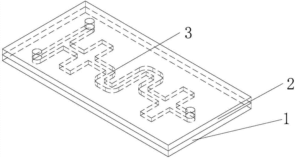
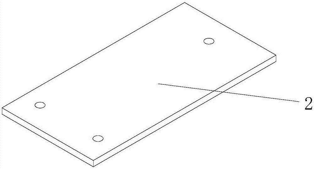
[0029] The microfluidic MEMS chip packaging method of this embodiment is used to package the upper substrate 2 with a microfluidic channel structure and the lower substrate 1 stacked and connected to the upper substrate 2 to obtain a microfluidic MEMS chip (see figure 1 ). The method includes the following steps:

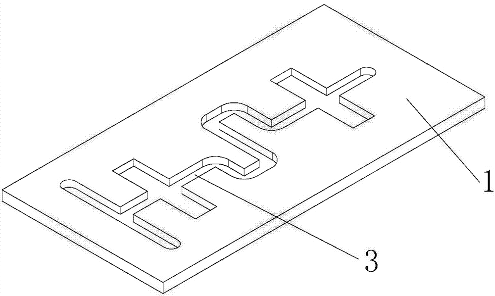
[0030] The first step is to prepare the lower substrate 1 (the lower substrate such as figure 2 shown)——Use the coating method (magnetron sputtering, evaporation or electroplating method) to coat a layer of metal film with a thickness of 200±50nm (preferably 200nm) on the upper surface of the lower substrate 1 made of glass, and use the MEMS process to coat the lower substrate 1 The micro-channel 3 is made on the metal film, and the pattern of the micro-channel 3 is designed according to the customer's requirements. The method for making the micro-flow channel 3 is as follows: after coating a metal masking material with a thickness of 2000 angstroms on the metal ...


PUM

PropertyMeasurementUnit
Softening pointaaaaaaaaaa

Abstract

The invention relates to a microfluidic MEMS chip packaging method, applied to packaging an upper substrate with a micro-channel structure and a lower substrate connected with the upper substrate in a stacking manner to acquire a microfluidic MEMS chip. The method comprises the following steps of 1, preparing the lower substrate; 2, preparing the upper substrate; 3, preparing the semi-finished chip; 4, pre-heating the semi-finished chip; and 5, bombarding the semi-finished chip by using a radio frequency power source. The microfluidic MEMS chip packaging method has the advantages that a radio frequency technology is used for acting on metal films on the upper and lower substrates, so that the surfaces of the metal films are partially subjected to high temperature, the surfaces of the substrates are melted with the metal films after melting, and thus the upper and lower substrates can be well tightly combined, bonding accuracy of a product is greatly improved, the micro-channel structure is prevented from being obstructed by a packaging process, a finished product ratio of chip packaging is improved, a production cycle is shortened, and production cost is reduced.

Description

technical field [0001] The invention relates to a MEMS chip radio frequency packaging method, in particular to a microfluidic MEMS chip packaging method, which belongs to the technical field of chip packaging. Background technique [0002] Microfluidic technology is one of the rapidly developing frontier fields of high-tech and interdisciplinary science and technology. It is an important technical platform for the research of signal detection and processing methods in biochemical detection, chemical science and information science. Microfluidic chips are based on MEMS (Micro Electro Mechanical Systems) processing technology, to study the surface properties of microfluidic channels, the driving and control laws in microfluidic systems, and to establish sample pretreatment, mixing, reaction, and separation. Microfluidic chip integration technology integrating functional units such as detection and detection. [0003] Microfluidic chips are one of the key devices in the fields...

Claims


Application Information

Patent Timeline
IPC IPC(8): B81C3/00B81C1/00
CPCB81C1/00269B81C3/001B81C2203/0118B81C2203/019B81C2203/036
Inventor 卫勇
Owner 镇江华瑞芯片科技有限公司
Why Eureka
Try Eureka