Display substrate and device

A technology for display substrates and display devices, used in semiconductor devices, electrical components, circuits, etc., can solve problems such as poor conductivity and affecting product yields

Inactive Publication Date: 2017-12-05
BOE TECH GRP CO LTD +1
View PDF3 Cites 12 Cited by
  • Summary
  • Abstract
  • Description
  • Claims
  • Application Information

AI Technical Summary

Problems solved by technology

When bonding the COF, the organic film is sandwiched between the signal line 12 and the COF. Since th

Method used


Image

  • Display substrate and device
  • Display substrate and device
  • Display substrate and device

Examples


Embodiment 1

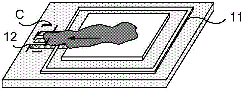
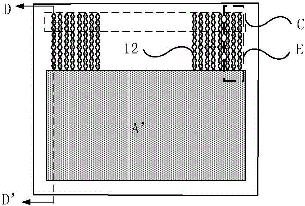
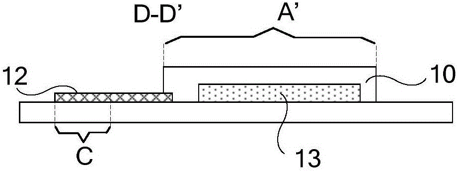
[0043] An embodiment of the present invention provides a display substrate, such as figure 2 with 3 As shown, it includes the display device 13 located in the encapsulation area A' of the display substrate, the signal line 12 extending from the encapsulation area A' of the display substrate to the non-encapsulation area, and the part covering the display device 13 and the signal line 12 located in the encapsulation area The thin film encapsulation layer 10. Among them, such as Figure 4 As shown, the part of the signal line 12 located in the non-packaging area has a first edge 121 and a second edge 122 opposite in the line width direction. The first edge 121 has protrusions and depressions that are alternately distributed in sequence toward the second edge 122 .

[0044] In this embodiment, the second edge 122 has protrusions and depressions facing the first edge 121 that are alternately distributed in sequence. Preferably, the second edge 122 can be as Figure 4 As show...

Embodiment 2

[0055] An embodiment of the present invention provides a display substrate, such as figure 2 with 3 As shown, it includes the display device 13 located in the encapsulation area A' of the display substrate, the signal line 12 extending from the encapsulation area A' of the display substrate to the non-encapsulation area, and the part covering the display device 13 and the signal line 12 located in the encapsulation area The thin film encapsulation layer 10. Among them, such as Figure 8 As shown, the part of the signal line 12 located in the non-packaging area has a first edge 121 and a second edge 122 opposite in the line width direction. The first edge 121 has protrusions and depressions which are alternately distributed in sequence towards the second edge 122 , and the second edge 122 is a straight line.

[0056] It should be noted that the shape of the first edge 121 of the signal line 12 is not limited. Optionally, the first edge 121 may be a triangular waveform, and...

Embodiment 3

[0061] An embodiment of the present invention provides a display substrate, such as figure 2 with 3 As shown, it includes the display device 13 located in the encapsulation area A' of the display substrate, the signal line 12 extending from the encapsulation area A' of the display substrate to the non-encapsulation area, and the part covering the display device 13 and the signal line 12 located in the encapsulation area The thin film encapsulation layer 10. Among them, such as Figure 5 As shown, the portion of the signal line 12 located in the non-packaging area A has a first edge 121 and a second edge 122 opposite to each other in the line width direction. The first edge 121 has protrusions and depressions that are alternately distributed in sequence toward the second edge 122 .

[0062] In this embodiment, the shape of the second edge 122 is consistent with that of the first edge 121 , and the line width of the portion of the signal line 12 located in the non-packaging ...


PUM


Abstract

The invention provides a display substrate and device, relates to the display technology field, aims to change the shape of a signal wire at a non-packaging area and further prolongs the time of organic solution flowing to a binding area of COF when an ink-jet printing method is utilized to make an organic film of a film packaging layer to reduce the reject ratio. The display substrate comprises a display device arranged at a packaging area of the display substrate, the signal wire extending from the packaging area of the display substrate to the non-packaging area, and the film packaging layer covering portions of the display device and the signal wire at the packaging area, wherein the portion of the signal wire at the non-packaging area has a first edge and a second edge which are opposite in the wire width direction, and the first edge has protruding and sunken parts which are sequentially alternately distributed and face the second edge.

Description

technical field [0001] The present invention relates to the field of display technology, in particular to a display substrate and a display device. Background technique [0002] Flexible OLED (Organic Light Emitting Diode, Organic Light Emitting Diode) can be bent or folded, because of its low power consumption, flexible use, fast response time, impact resistance, strong shock resistance, light weight, easy to carry, etc., it has become more and more popular. more and more widely used. [0003] Flexible OLED usually adopts a thin film encapsulation process. The thin film encapsulation layer (English name: Thin filmencapsulation, English abbreviation: TFE) includes two layers of inorganic films and an organic film between the two layers of inorganic films. The film encapsulation layer can prevent water vapor from intruding into the display device. Thereby preventing failure of the display device. Among them, the preparation method of the organic thin film is as follows: Fir...

Claims


Application Information

Patent Timeline
IPC IPC(8): H01L27/32
CPCH10K59/131
Inventor 肖昂刘江
Owner BOE TECH GRP CO LTD
Why Eureka
Try Eureka