

Film transistor structure and AMOLED driving circuit
A technology of thin film transistors and oxide semiconductors, which is applied in the direction of transistors, circuits, electrical components, etc., can solve the problems of poor working stability of thin film transistors, improve working stability, solve poor working stability, and improve screen display quality Effect
- Summary
- Abstract
- Description
- Claims
- Application Information
AI Technical Summary
Problems solved by technology
Method used
Image

Examples
Embodiment Construction
[0063] The following will clearly and completely describe the technical solutions in the embodiments of the present invention in conjunction with the accompanying drawings in the embodiments of the present invention. Obviously, the described embodiments are only some of the embodiments of the present invention, not all of them. Based on the embodiments of the present invention, all other embodiments obtained by persons of ordinary skill in the art without making creative efforts belong to the protection scope of the present invention.
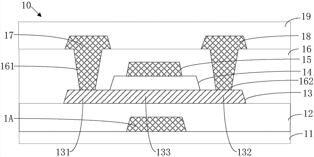
[0064] Please refer to figure 1 , figure 1 It is a structural schematic diagram of an embodiment of the thin film transistor structure of the present invention. The thin film transistor structure 10 of this embodiment includes a thin film substrate 11, a buffer layer 12, a metal oxide semiconductor layer 13, a gate insulating layer 14, a gate metal layer 15, an interlayer insulating layer 16, a source metal layer 17, a drain metal layer 18 an...
PUM
| Property | Measurement | Unit |
|---|---|---|
| Thickness | aaaaa | aaaaa |
Abstract
Description
Claims
Application Information