Masking apparatus for cathode ring repair and method of use thereof

A cathode ring and mask technology, which is applied in the direction of semiconductor devices, electrical components, circuits, etc., can solve problems such as open circuit failure, poor contact, and inability to solve black spot defects, so as to ensure light output, ensure process compatibility, and avoid black spots. The effect of point defects

Active Publication Date: 2020-05-05
南京睿显电子科技有限公司
View PDF3 Cites 0 Cited by
  • Summary
  • Abstract
  • Description
  • Claims
  • Application Information

AI Technical Summary

Problems solved by technology

Due to the large difference in thickness, it often leads to breakage and poor contact when the edge step of the anode metal layer contacts the semi-transparent cathode layer, which causes the device drive voltage to increase or open circuit failure
However, simply thickening the metal cathode layer will lead to a significant decrease in the light output of the device.
[0003] At present, adding a layer of transparent conductive layer (ITO) on the cathode layer by sputtering can solve the problem of cathode fracture, but the sputtering method itself will generate a large number of high-speed particles impacting the surface of the device, causing black spot defects, and greatly reducing the yield
However, all transparent conductive films currently used are prepared by sputtering due to their high evaporation temperature, which cannot solve the problem of black spot defects.

Method used


Image

  • Masking apparatus for cathode ring repair and method of use thereof
  • Masking apparatus for cathode ring repair and method of use thereof
  • Masking apparatus for cathode ring repair and method of use thereof

Examples


Embodiment Construction

[0024] In order to have a clearer understanding of the technical features, purposes and effects of the present invention, the specific implementation manners of the present invention will now be described in detail with reference to the accompanying drawings.

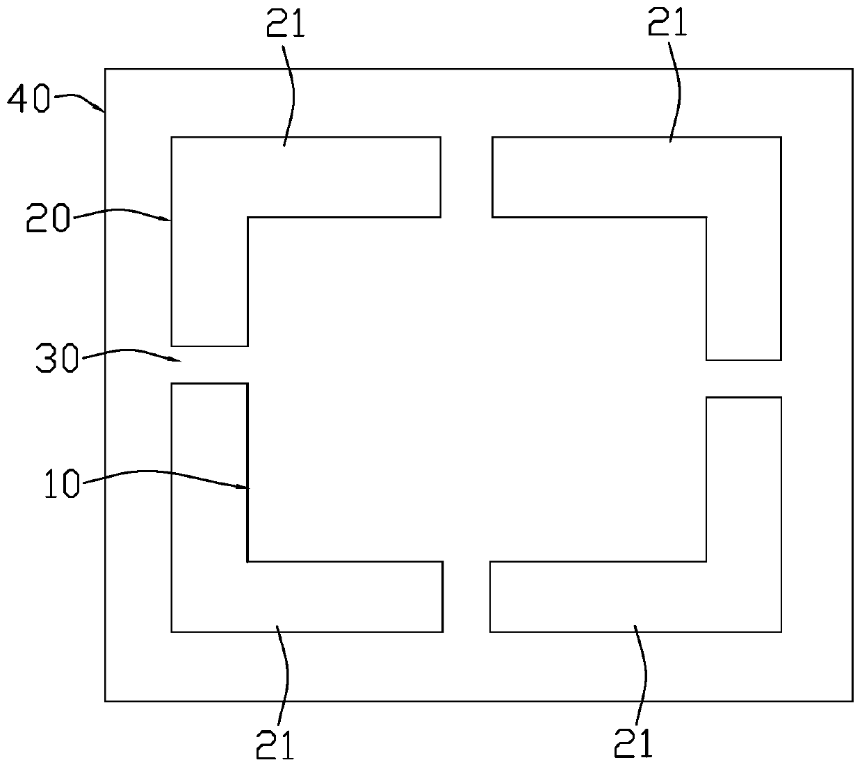
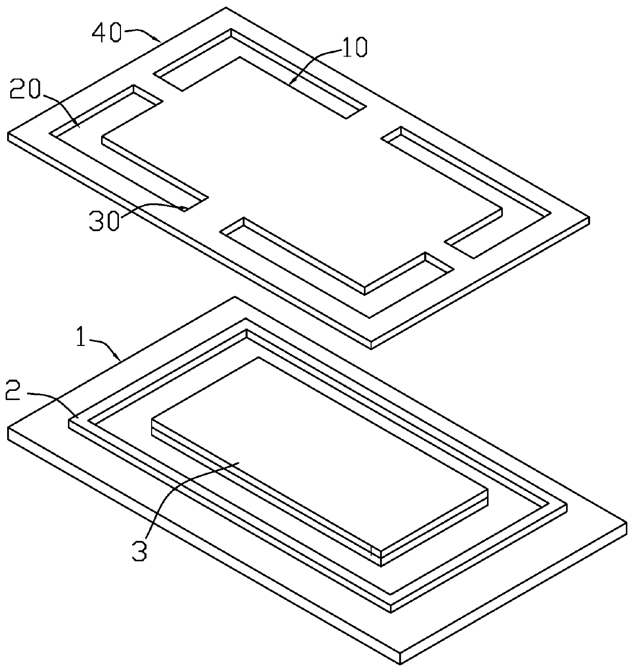
[0025] Such as figure 1 As shown, the mask device for cathode ring repair according to an embodiment of the present invention includes a mask, and the mask includes a display area shielding part 10, a hollow part 20 and a rib 30, and the hollow part 20 is connected by the rib 30 on the periphery of the display area shielding portion 10 .

[0026] When the cathode ring is repaired, the mask plate is set above the device where the cathode ring is located.

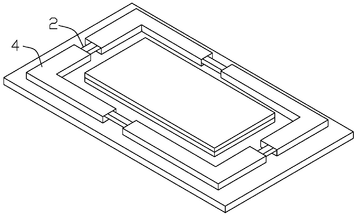
[0027] combine figure 1 , 2 , in a display 1 such as an OLED microdisplay, the cathode ring 2 is located at the periphery of the display area 3 on the display 1 . In the mask plate of the present invention, the display area shielding part 10 is directly facing the ...


PUM


Abstract

The invention discloses a mask device for cathode ring repair and its application method. The mask device includes a mask, and the mask includes a display area shielding part, a hollow part and a reinforcing rib, and the hollow part passes through The reinforcing rib is connected to the periphery of the display area shielding part. The mask device of the present invention is used for shielding protection when the cathode ring is repaired, preventing the repair material of the cathode ring from entering the display area of ​​the device and affecting the photoelectric performance of the device such as brightness and display uniformity, and avoiding the use of sputtering to prepare metal oxidation. The black spot defects caused by the material transparent conductive protective layer can be used to achieve cathode ring protection by using various PVD processes such as sputtering and evaporation, which ensures the light output and process compatibility of the device to the greatest extent.

Description

technical field [0001] The invention relates to a mask device for repairing cathode rings, in particular to a mask device suitable for repairing cathode rings of OLED microdisplays and a method for using the same. Background technique [0002] In the production and preparation process of OLED microdisplays, a top-emitting light-emitting device structure is generally used, and its anode usually adopts a thick metal layer to ensure high reflectivity. preparation, while the cathode is prepared with a very thin layer of thermal evaporation to ensure the light output A translucent metal layer is achieved. Due to the large difference in thickness, it often leads to breakage and poor contact between the edge step of the anode metal layer and the semi-transparent cathode layer, which causes the device driving voltage to increase or open circuit failure. However, simply thickening the metal cathode layer will lead to a significant decrease in the light output of the device. [0...

Claims


Application Information

Patent Timeline
Patent Type & Authority Patents(China)
IPC IPC(8): H01L51/56H01L51/52
CPCH10K50/82H10K71/00
Inventor 茆胜
Owner 南京睿显电子科技有限公司
Why Eureka
Try Eureka