Unlock instant, AI-driven research and patent intelligence for your innovation.

Thin film transistor manufacturing method, TFT array substrate and flexible display screen

A technology of thin film transistors and manufacturing methods, which is applied in the fields of thin film transistor manufacturing methods, TFT array substrates and flexible display screens, and can solve problems such as broken gate insulating layers

Active Publication Date: 2017-12-08
SHENZHEN ROYOLE TECH CO LTD
View PDF2 Cites 2 Cited by
  • Summary
  • Abstract
  • Description
  • Claims
  • Application Information

AI Technical Summary

Problems solved by technology

[0003] Embodiments of the present invention provide a method for manufacturing a thin film transistor and an array substrate, which are used to solve the technical problem that the climbing structure with a height difference in the gate insulating layer is broken when it is stressed and affects other layer structures

Method used


Image

  • Thin film transistor manufacturing method, TFT array substrate and flexible display screen
  • Thin film transistor manufacturing method, TFT array substrate and flexible display screen
  • Thin film transistor manufacturing method, TFT array substrate and flexible display screen

Examples


Embodiment Construction

[0017] The following will clearly and completely describe the technical solutions in the embodiments of the present invention with reference to the drawings in the embodiments of the present invention.

[0018] The invention provides a thin film transistor, a TFT array substrate and a flexible display screen, and the thin film transistor can be used in a liquid crystal display screen or an organic display screen. The flexible display screen involved in the embodiment of the present invention is used for but not limited to mobile phone, tablet computer, palmtop computer, personal digital assistant (Personal Digital Assistant, PDA) or e-reader, etc., which is not specifically limited in the embodiment of the present invention.

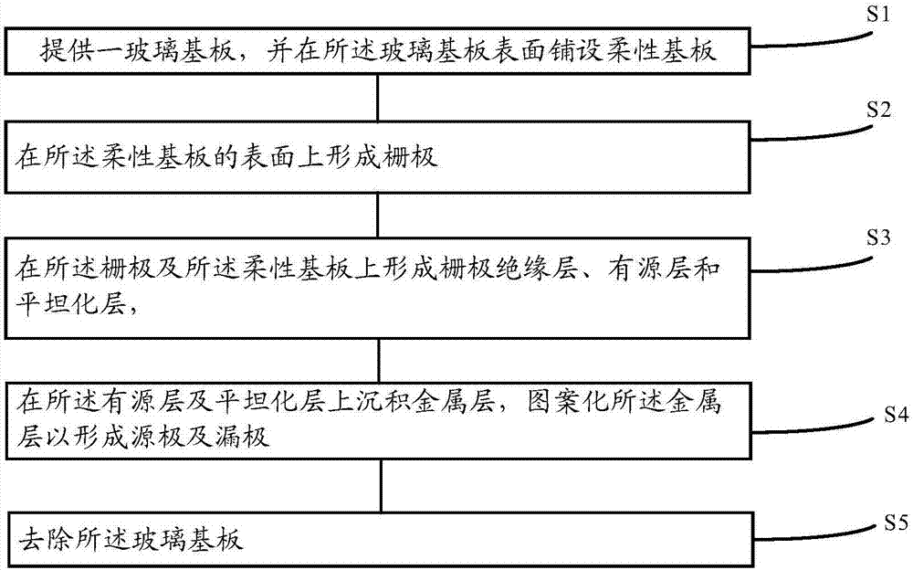
[0019] The invention provides a method for manufacturing a thin film transistor, the method comprising:

[0020] forming a gate on a flexible substrate;

[0021] Forming a gate insulating layer, an active layer and a planarization layer on the gate and ...


PUM


Abstract

The present invention provides a thin film transistor manufacturing method and a TFT array substrate. The TFT array substrate includes a flexible substrate 10, a gate 12 stacked on a surface of the flexible substrate 10, a gate insulating layer covering the gate 12, 14), an active layer (16) stacked on the gate insulating layer (14), a planarization layer provided on the surface of the flexible substrate (10) and located at two opposite sides of the gate insulating layer A source electrode and a drain electrode, the planar layer being connected to the gate insulating layer, the source electrode and the drain electrode being both formed, On the active layer (16) and the planarization layer (18); and the source (19) and the drain (20) are disposed at intervals. Also provides a flexible display.

Description

technical field [0001] The invention relates to the field of manufacturing thin film transistors, in particular to a method for manufacturing thin film transistors, a TFT array substrate and a flexible display screen. Background technique [0002] At present, thin-film transistor (Thin-film transistors, TFT) array substrates are widely used in different types of display devices, such as flexible display screens, LCD or OLED display screens. A high-quality gate insulating layer in a thin film transistor is the key to achieving important parameters such as good electrical stability and small leakage current of the TFT array substrate. Therefore, the gate insulating layer is usually made of inorganic materials, such as using SiNx or SiOx through Chemical vapor deposition forms. When the TFT array substrate is applied to a flexible display, as the flexible substrate bends, the TFT film layer structure on it will be subjected to tensile stress and compressive stress correspondin...

Claims


Application Information

Patent Timeline
IPC IPC(8): H01L21/336H01L27/12
CPCH01L27/1214H01L27/127H01L29/66742H01L29/786
Inventor 赵继刚袁泽余晓军魏鹏
Owner SHENZHEN ROYOLE TECH CO LTD
Features
  • R&D
  • Intellectual Property
  • Life Sciences
  • Materials
  • Tech Scout
  • Unparalleled Data Quality
  • Higher Quality Content
  • 60% Fewer Hallucinations
Learn More