Peripheral circuit structure of array substrate

A peripheral circuit and array substrate technology, applied in the field of peripheral circuit structure, can solve serious problems, adverse effects of HVA process, RC delay, etc., to achieve the effect of improving yield, improving curing effect, and reducing RC load

Active Publication Date: 2017-12-12
TCL CHINA STAR OPTOELECTRONICS TECH CO LTD
View PDF6 Cites 7 Cited by
  • Summary
  • Abstract
  • Description
  • Claims
  • Application Information

AI Technical Summary

Problems solved by technology

However, the disadvantage of this circuit structure is: since only the left array test pad 3a is electrically connected to the HVA process line 2, the entire panel can only be processed by sending signals from one side during the HVA process.
When the panel size is large, the RC delay is very serious, which will adversely affect the HVA process

Method used


Image

  • Peripheral circuit structure of array substrate
  • Peripheral circuit structure of array substrate
  • Peripheral circuit structure of array substrate

Examples


Embodiment 1

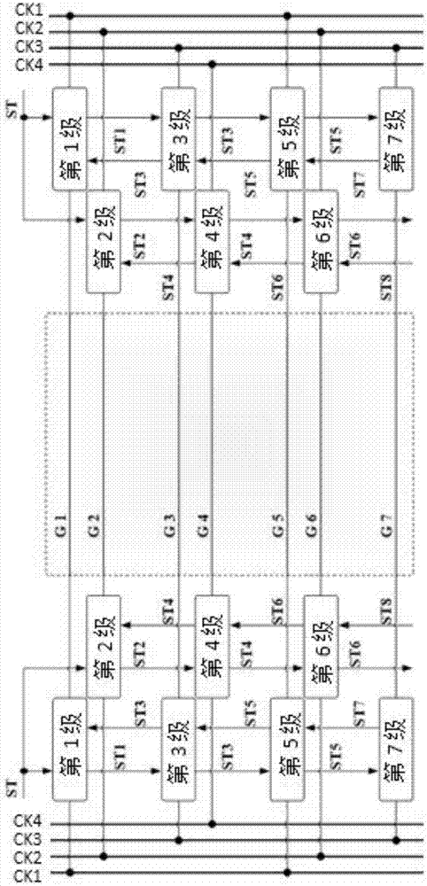
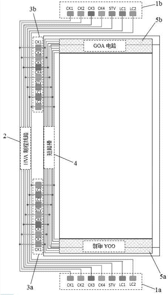
[0038] This embodiment provides a peripheral circuit structure of an array substrate, refer to Figure 4 and Figure 5 , the array substrate 10 includes a display area 11 and a fan-out area 12 located at the edge of the display area 11 , and the peripheral circuit structure is arranged on the fan-out area 12 .

[0039] Specifically, the peripheral circuit structure includes: first GOA circuit 20a and first array test pad 30a electrically connected to each other, second GOA circuit 20b and second array test pad 30b electrically connected to each other, HVA process Line 40. The first array of test pads 30a is connected to the HVA process line 40 through a first connection line 50a, and the second array of test pads 30b is connected to the HVA process line 40 through a second connection line 50b. In this embodiment, the first GOA circuit 20a and the second GOA circuit 20b are respectively located on the first side 11a and the second side 11b opposite to the display area 11, and...

Embodiment 2

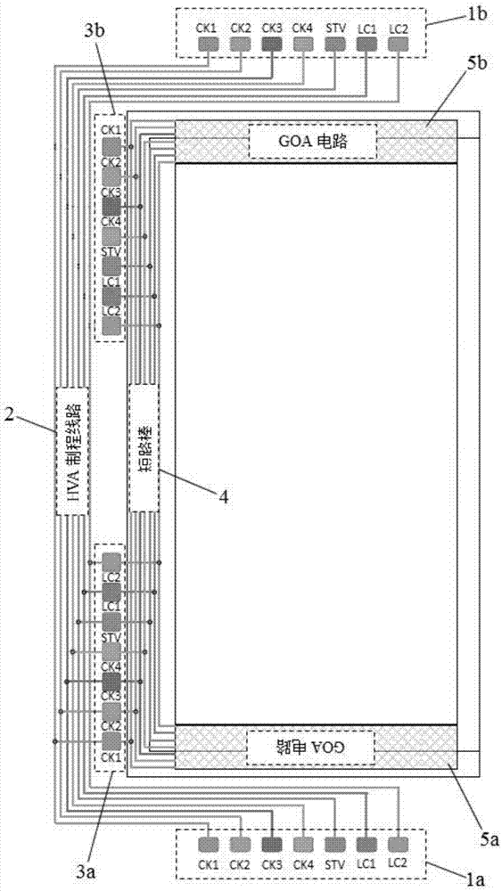
[0047] The difference between this embodiment and embodiment 1 is that, refer to Figure 10 and Figure 11 , the circuit breaking point 80 is set on the HVA process line 40, the HVA process line 40 is divided into a first line segment 40a and a second line segment 40b insulated from each other to form the circuit break point 80, the The welding point 81 is arranged above the circuit breaking point 80 , and after the welding process is performed at the welding point 81 , the first line section 40 a and the second line section 40 b are electrically connected to each other. In this embodiment, the first array test pad 30a is electrically connected to the first line segment 40a, and the second array test pad 30b is electrically connected to the second line segment 40b. The specific connection The structure can refer to the embodiment 1 Figure 7 structure shown. Other circuit structures in this embodiment are the same as those in Embodiment 1, and will not be repeated here.

...


PUM


Abstract

The invention discloses a peripheral circuit structure of array substrate, the peripheral circuit structure includes a first GOA circuit, a first array test pads, a second GOA circuit, a second array test pads, and an HVA process line; the first array test pads and the second array test pads are respectively connected to the HVA process line through a first connecting line and a second connecting line, wherein a circuit breakpoint is arranged on a circuit line formed by connecting the first array test pads to the second array test pads through a first connecting line, an HVA process line and a second connecting line in sequence and is preset with a welding point which is used to electrically connect the circuit breakpoints after a welding procedure is carried out. The peripheral circuit structure has the advantages that the separate tests for the two GOA circuits are achieved, thus avoiding the occurrence of the leak detection and additionally that a dual drive mode is further adopted in the HVA process helps to improve the curing effect of the HVA process.

Description

technical field [0001] The present invention relates to the technical field of displays, in particular to a peripheral circuit structure of an array substrate. Background technique [0002] Among the existing display panel technologies, GOA (Gate-driver On Array) technology has been widely used in liquid crystal panel design because it can reduce the size of the panel frame and has the advantage of reducing costs. [0003] Since the GOA circuit is composed of a-Si TFT devices, and the driving capability of a-Si TFT devices is relatively weak, large-size GOA display panels generally adopt a double-sided driving design. figure 1 It is a schematic diagram of the architecture of a bilaterally driven GOA liquid crystal display panel, which is a schematic diagram of a GOA circuit with four clock signals (CK1 to CK4). lie in figure 1 The dotted frame in the middle indicates the display area of ​​the liquid crystal display panel. Level 1 to level 7 in the figure respectively repr...

Claims


Application Information

Patent Timeline
Patent Type & Authority Applications(China)
IPC IPC(8): G02F1/1362G02F1/1345
CPCG02F1/13454G02F1/1362G02F1/136286G02F1/136254
Inventor 杜鹏
Owner TCL CHINA STAR OPTOELECTRONICS TECH CO LTD
Why Eureka
Try Eureka