
A carrying device and a pre-cleaning chamber
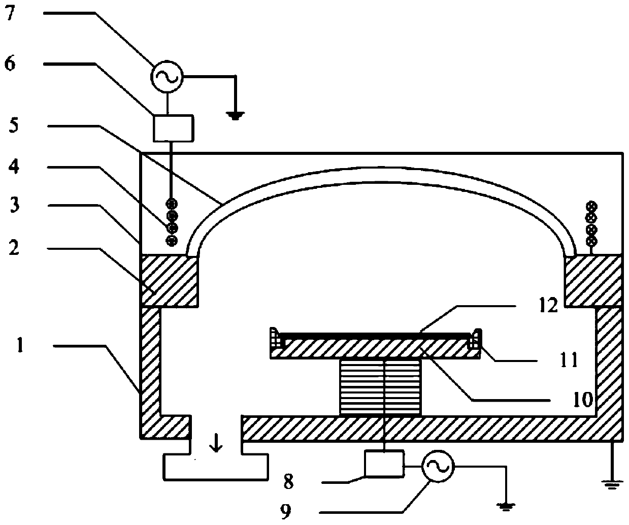
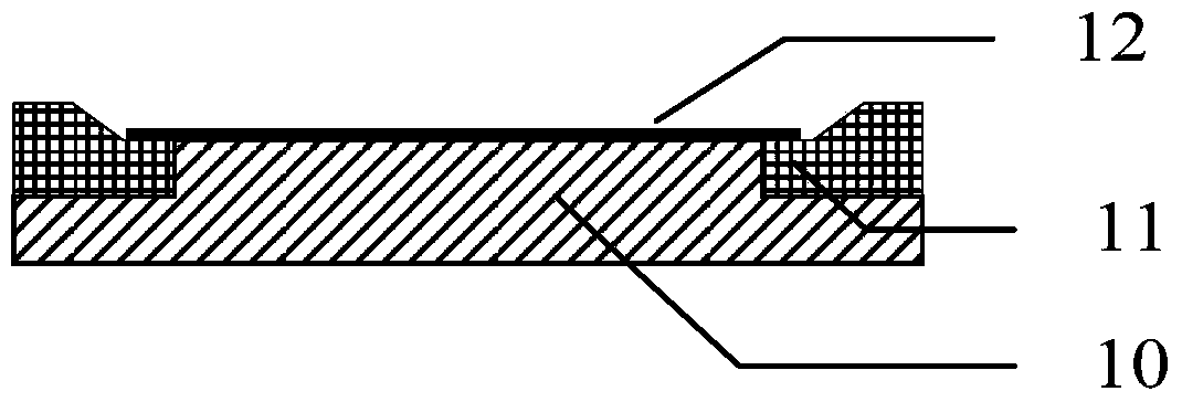
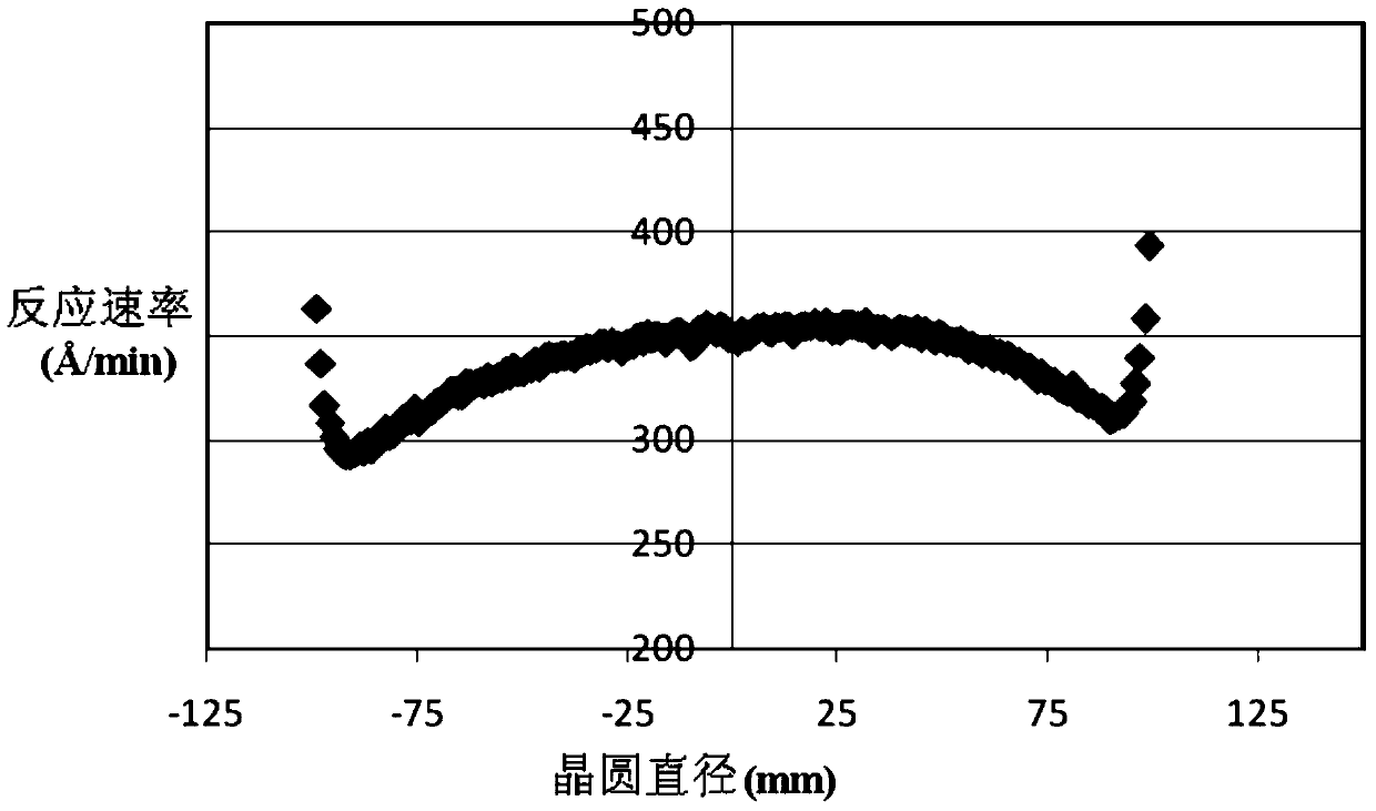
A technology of a carrying device and a ring piece, which is applied in the directions of vacuum evaporation plating, coating, discharge tube, etc., can solve the problems of uneven distribution of the radial etching rate of the metal disc 10, affecting the etching uniformity of the wafer 12, etc. , to achieve the effect of improving etching uniformity and uniform plasma density distribution
- Summary
- Abstract
- Description
- Claims
- Application Information
AI Technical Summary
Problems solved by technology
Method used
Image

Examples
Embodiment 1
[0049] This embodiment provides a carrying device, the carrying device includes a top plate for carrying workpieces to be processed, the top plate includes a central piece and an annular piece surrounding the central piece, and the central piece and the annular piece are insulated from each other;
[0050] By loading different negative bias voltages to the center piece and the ring piece respectively, the etching rates at different positions in the radial direction of the workpiece to be processed tend to be consistent.
[0051] Different negative biases are loaded on the central part and the ring part of the carrying device in this embodiment, so that the plasma density distribution on the workpiece to be processed carried by the carrying device is uniform, so that the workpiece to be processed can be marked at different positions in the radial direction. The etching rate tends to be consistent, thereby improving the etching uniformity on the workpiece to be processed.
Embodiment 2
[0053] Such as Figure 4 , 5 As shown, the present embodiment provides a carrying device, the carrying device includes a top plate for carrying workpieces to be processed, the top plate includes a central piece 14 and an annular piece 15 surrounding the central piece 14, and the central piece 14 and the annular piece 15 Mutual insulation;
[0054] By loading different negative bias voltages on the central piece 14 and the ring piece 15 respectively, the etching rates at different positions of the workpiece to be processed in the radial direction tend to be consistent.
[0055] The central part 14 and the annular part 15 of the carrier device in this embodiment are loaded with different negative bias voltages, so that the plasma density distribution on the workpiece to be processed carried by the carrier device is uniform, so that the workpiece to be processed is in different positions in its radial direction. The etch rate tends to be consistent, thereby improving the etch u...
Embodiment 3
[0078] Such as Figure 6 , 7 As shown, the present embodiment provides a carrying device, and the difference from Embodiment 2 is:
[0079] The voltage adjustment module in this embodiment includes a central submodule and an edge submodule, wherein,
[0080] The central sub-module is used to load the first DC positive voltage to the central part 14;
[0081] The edge sub-module is used to load the ring 15 with a second positive DC voltage; and, the second positive DC voltage is smaller than the first positive DC voltage.
[0082] It should be noted that the number of rings 15 in this embodiment is multiple and nested with each other, and two adjacent rings 15 are insulated from each other;
[0083] The number of edge sub-modules corresponds to the number of rings 15, and each edge sub-module applies a different second DC positive voltage to each ring 15 one by one, and the closer the ring 15 is to the edge, the loaded second DC positive voltage is smaller.
[0084] It sho...
PUM
 Abstract
Description
Claims
Application Information