Making method for grid structure

A manufacturing method and gate structure technology, applied in the direction of semiconductor devices, etc., can solve the problems of increasing gates, device performance degradation, device failure, etc., to suppress the generation of gate root defects, uniform etching rate, and shorten the time interval Effect

Active Publication Date: 2009-09-09
SEMICON MFG INT (SHANGHAI) CORP +1
View PDF4 Cites 0 Cited by
  • Summary
  • Abstract
  • Description
  • Claims
  • Application Information

AI Technical Summary

Problems solved by technology

Then, the root defect of the barrier layer will serve as a hard mask for etching the conductive layer and the dielectric layer at the same time, so that the etching gas cannot etch the conductive layer and the dielectric layer under the root defect of the barrier layer, forming a gate root defect
The existence of the root defect of the gate is equivalent to increasing the length of the gate, and the increase of the gate length is likely to cause a decrease in device performance, such as a decrease in drain saturation current, a decrease in threshold voltage, and an increase in interjunction capacitance. will cause device failure

Method used


Image

  • Making method for grid structure
  • Making method for grid structure
  • Making method for grid structure

Examples


no. 3 example

[0061] As the third embodiment of the method of the present invention, its specific implementation steps include:

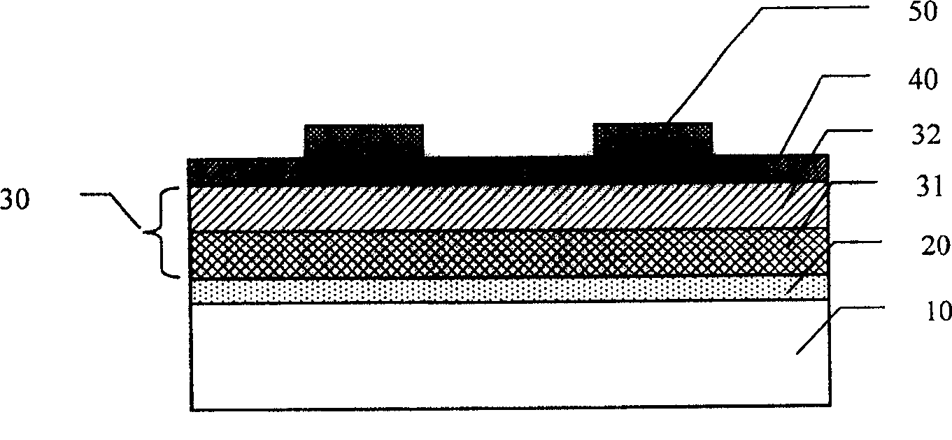
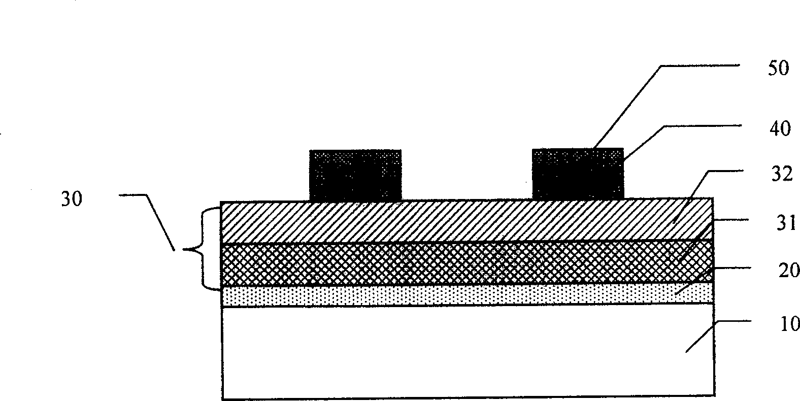
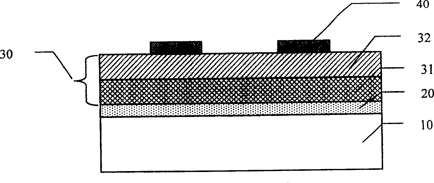
[0062] Firstly, a dielectric layer, a conductive layer, a barrier layer and a patterned photoresist layer are sequentially deposited on the substrate. Wherein, the conductive layer includes a polysilicon layer and a metal layer deposited sequentially.

[0063] Then, using the patterned photoresist layer as a mask, the blocking layer is etched to obtain a blocking layer with an opening area; the opening area of ​​the blocking layer exposes the upper surface of the metal layer.

[0064] Afterwards, the patterned photoresist layer is removed to obtain a smooth upper surface of the barrier layer and the metal layer.

[0065] Subsequently, the metal oxide is etched using the barrier layer with the opening region as a mask.

[0066] As an embodiment of the method of the present invention, the time interval between the removal of the patterned photoresist layer and th...


PUM


Abstract

A method for manufacturing a gate structure, comprising: sequentially depositing a dielectric layer, a conductive layer, a barrier layer, and a patterned photoresist layer on a substrate; etching the barrier layer; removing the patterned photoresist The etchant layer: using the first etching gas to etch the upper surface of the conductive layer; using the second etching gas to etch the conductive layer and the dielectric layer. By respectively setting the etching rates of the etching gas on the conductive layer material and the metal layer material oxide on the conductive layer, a certain etching selectivity ratio of the etching gas to the conductive layer material and the metal layer material oxide can be obtained, and finally no Gate structure with root defects.

Description

technical field [0001] The invention relates to the technical field of semiconductor manufacturing, in particular to a method for manufacturing a gate structure. Background technique [0002] Semiconductor devices change the electric field strength in the dielectric layer by applying a voltage on the gate, and then control the electric field on the surface of the substrate, and finally change the conductivity of the conductive channel. It can be seen that the performance of the gate is very important to the performance of the semiconductor device, and the performance of the gate is mainly determined by the structure of the gate. [0003] Figure 1A-1D In order to illustrate the device cross-sectional diagram of each step of the manufacturing method of the gate structure in the prior art, as shown in the figure, a manufacturing method of the gate structure provided in the Chinese patent application with the application number "CN97111174.X" is as follows: [0004] First, if ...

Claims


Application Information

Patent Timeline
Patent Type & Authority Patents(China)
IPC IPC(8): H01L21/28
Inventor 罗飞吴金刚高大为高关且
Owner SEMICON MFG INT (SHANGHAI) CORP
Why Eureka
Try Eureka