Anti-attaching plate

An anti-sticking and anti-sticking technology, which is applied in the direction of ion implantation plating, metal material coating process, coating, etc., can solve the problems of increased pressure and affecting cleaning, so as to reduce warpage and solve warpage The effect of increasing and releasing the stress of the film layer

Inactive Publication Date: 2017-12-15
SHENZHEN CHINA STAR OPTOELECTRONICS SEMICON DISPLAY TECH CO LTD
View PDF3 Cites 4 Cited by
  • Summary
  • Abstract
  • Description
  • Claims
  • Application Information

AI Technical Summary

Problems solved by technology

However, it is necessary to thicken the conductive metal film layer to meet the needs of the panel response speed; and thickening the metal film layer will lead to increased pressure
[0005] During the vacuum sputtering deposition process, the sputtered target atoms or large-sized particles will eventually fly to the inner wall surface of the sputtering machine, affecting its cleaning

Method used


Image

  • Anti-attaching plate
  • Anti-attaching plate
  • Anti-attaching plate

Examples


Embodiment Construction

[0025] The following description of the embodiments refers to the accompanying drawings to illustrate specific embodiments in which the invention may be practiced. The directional terms mentioned in the present invention, such as "up", "down", "front", "back", "left", "right", "top", "bottom", etc., are only for reference to the attached drawings. direction. Therefore, the directional terms used are used to illustrate and understand the present invention, but not to limit the present invention.

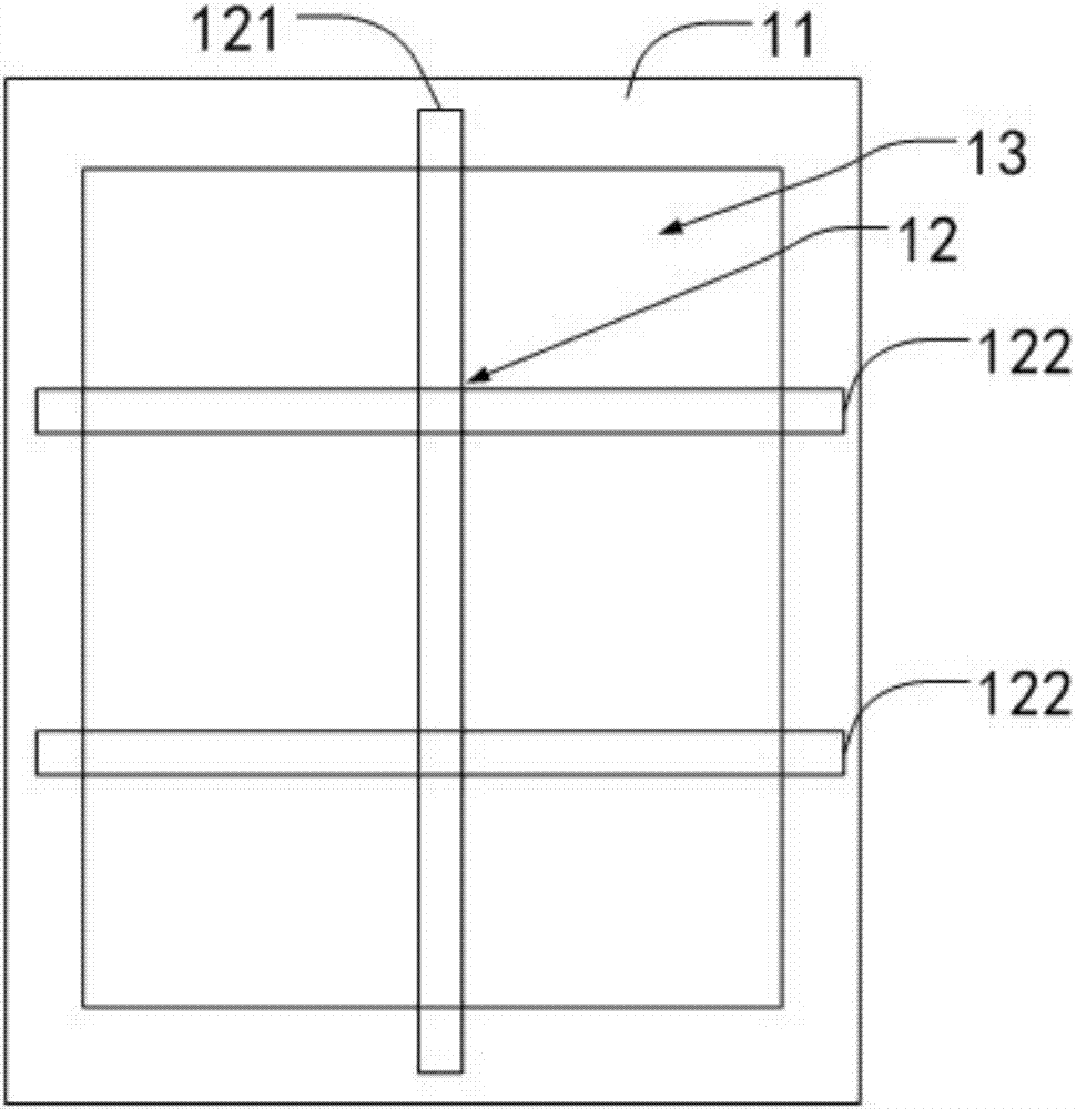
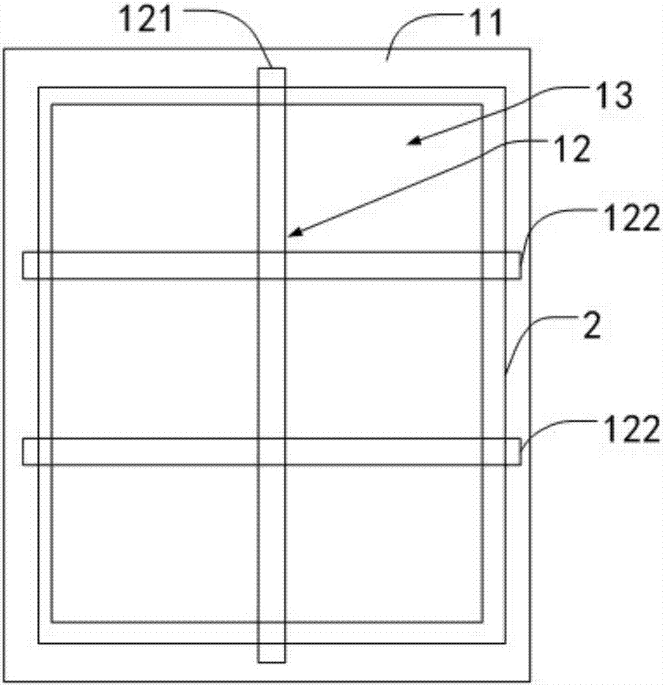
[0026] Examples such as figure 1 As shown, an anti-slip board includes a motherboard 11 and an anti-strip 12 .

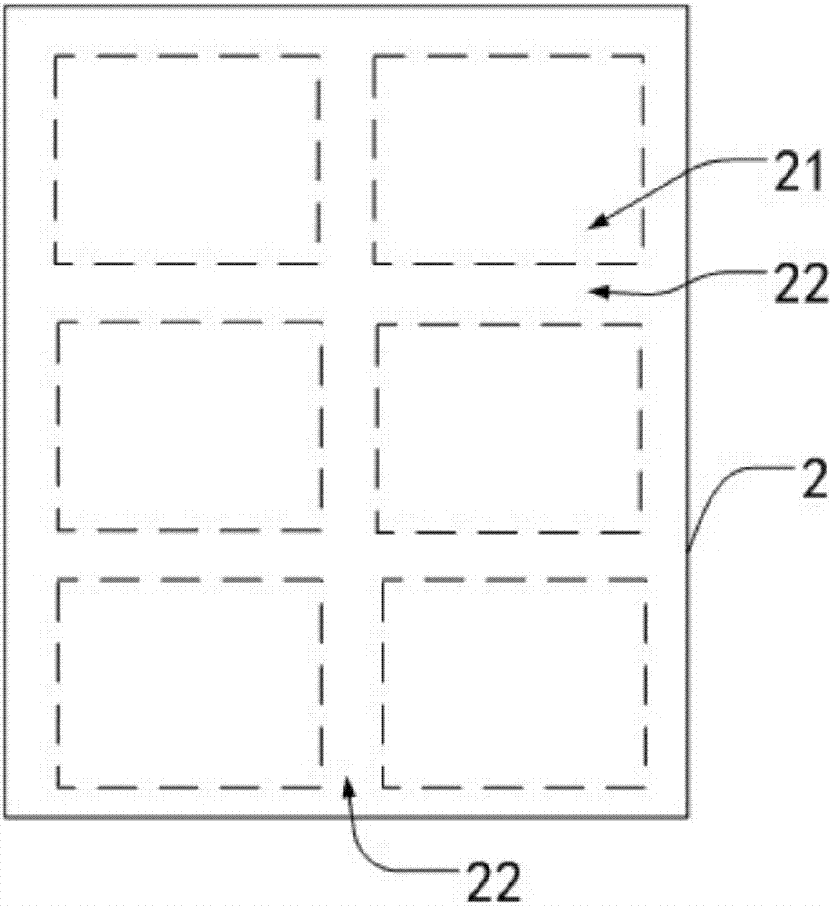
[0027] In this embodiment, a sputtering zone is provided in the middle of the motherboard 11 ; the anti-strips 12 are assembled on the motherboard 11 and divide the sputtering zone into a plurality of independent sputtering zones 13 .

[0028] Wherein, in this embodiment, the anti-stripping strip 12 includes a first strip body 121 and a second strip body 122, and the fir...


PUM

PropertyMeasurementUnit
widthaaaaaaaaaa

Abstract

The invention discloses an anti-attaching plate which comprises a base plate and anti-attaching strips. The base plate is provided with a sputtering area. The anti-attaching strips are assembled to the base plate and divide the sputtering area into multiple mutually-independent sputtering subareas. The base plate is provided with mutually-separated film deposition areas, each sputtering subarea corresponds to one film deposition area, and the anti-attaching strips correspond to the gaps between the film deposition areas. When sputtering and film forming are carried out on the base plate, target materials are deposited on the film deposition areas through the sputtering subareas and form film layers.

Description

technical field [0001] The invention relates to the fields of films and the like, in particular to an anti-sticking board. Background technique [0002] With the development of large-size panels, the warpage of the glass substrate will also increase accordingly. [0003] The warpage of the glass substrate becomes larger, and the suction cup on the robotic arm cannot completely suck it during the transfer process, resulting in an increased risk of fragmentation. [0004] When the glass substrate with large warpage after film formation is patterned through the yellow light process and etching process, the stress of the film layer is released and the warpage is reduced. However, it is necessary to thicken the conductive metal film layer to meet the requirements of the response speed of the panel; and thickening the metal film layer will lead to an increase in pressure. [0005] During the process of vacuum sputtering deposition, the sputtered target atoms or large-sized parti...

Claims


Application Information

Patent Timeline
Patent Type & Authority Applications(China)
IPC IPC(8): C23C14/34C23C14/04
CPCC23C14/34C23C14/042
Inventor 胡小波
Owner SHENZHEN CHINA STAR OPTOELECTRONICS SEMICON DISPLAY TECH CO LTD
Why Eureka
Try Eureka