Light emitting diode chip scale packaging structure

一种发光二极管、芯片级封装的技术,应用在半导体器件、电气元件、电路等方向,能够解决光学不良等问题

Active Publication Date: 2017-12-19
LEXTAR ELECTRONICS CORP
View PDF2 Cites 4 Cited by
  • Summary
  • Abstract
  • Description
  • Claims
  • Application Information

AI Technical Summary

Problems solved by technology

However, it is difficult for the refractive lens to break through its physical threshold limit when designing at a lower thickness
In addition, due to the problem of the accuracy of the parts, the assembly of the overall module often causes poor optics due to the deviation of the parts.

Method used


Image

  • Light emitting diode chip scale packaging structure
  • Light emitting diode chip scale packaging structure
  • Light emitting diode chip scale packaging structure

Examples


Embodiment Construction

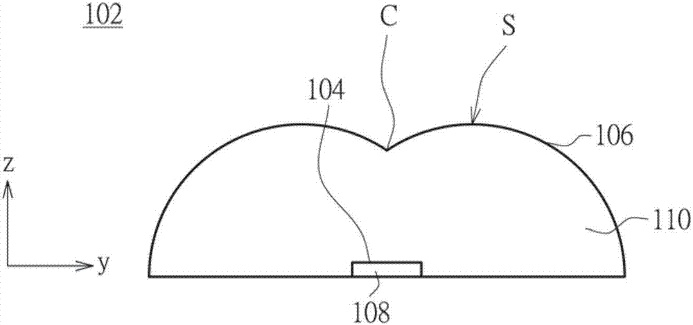
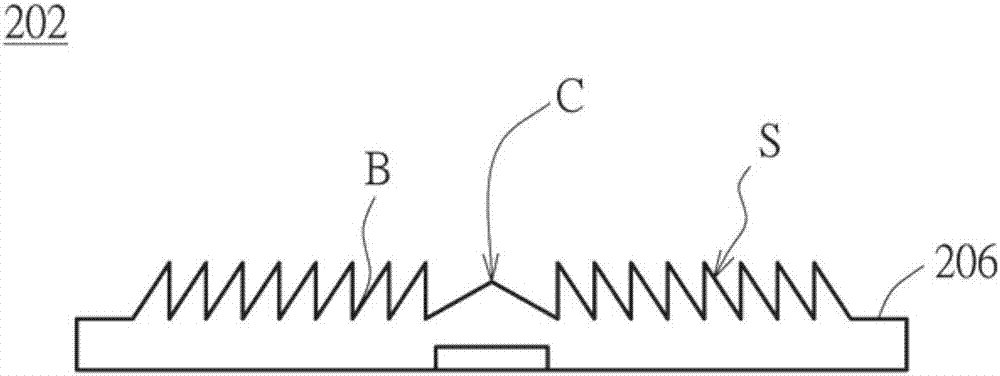
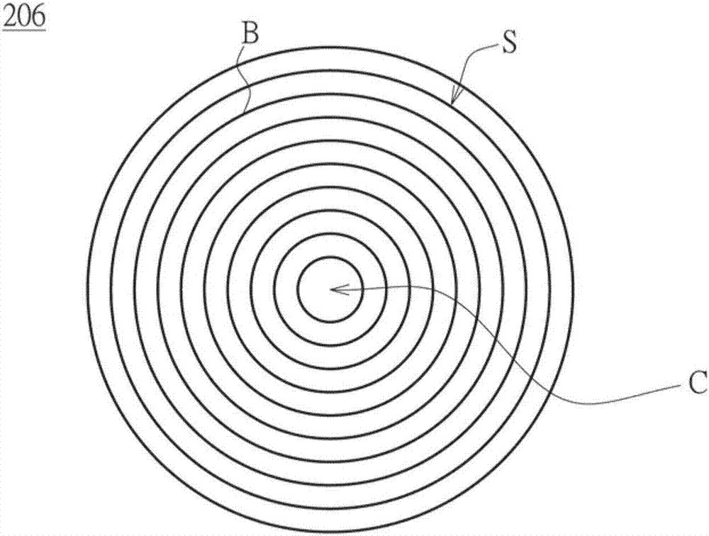
[0061] The embodiments of the summary of the invention provide a LED packaging structure, such as a LED chip-scale packaging structure, a light emitting device including the LED packaging structure, and a manufacturing method thereof. The light-emitting diode packaging structure can provide excellent lighting and display effects.

[0062] It should be noted that the present invention does not show all possible embodiments, and other implementations not presented in the present invention may also be applicable. Furthermore, the size ratios on the drawings are not drawn to the same scale as the actual product. Therefore, the specification and illustrations are only used to describe the embodiments, not to limit the protection scope of the present invention. In addition, the descriptions in the embodiments, such as detailed structures, manufacturing process steps and material applications, etc., are for illustration purposes only, and are not intended to limit the protection sco...


PUM


Abstract

A center point of the curve corresponding to the light emitting diode chip is a zero point of y-z coordinate axes. z is a variable of vertical axis of the curve. y is a variable of horizontal axis of the curve. ai is a constant coefficient in a term of ith degree. 3<n<=6.

Description

technical field [0001] The invention relates to a light emitting diode packaging structure, and in particular to a light emitting diode packaging structure with a lens. Background technique [0002] Since Light-Emitting Diodes (LEDs) have the advantages of long life, small size, low vibration, low heat dissipation, and low energy consumption, LEDs have been widely used in devices such as indicator lights or home light sources. In recent years, with the development of multi-color gamut and high brightness, light-emitting diodes have been applied in various display devices, illumination devices, and the like. [0003] The light-emitting properties of the device will affect the display performance of the product. [0004] For example, a liquid crystal display device uses a backlight module. The direct-lit backlight module can be used with LED light sources and lenses. [0005] One solution of the direct-type light-emitting module is to use a reflective lens, which can direct...

Claims


Application Information

Patent Timeline
Patent Type & Authority Applications(China)
IPC IPC(8): H01L33/52H01L33/54H01L33/58
CPCH01L33/52H01L33/54H01L33/58H01L33/502H01L2933/0058H01L2933/005H01L33/20H01L33/50H01L27/156
Inventor 黄哲瑄张书修苏信纶林志豪蔡宗良
Owner LEXTAR ELECTRONICS CORP
Why Eureka
Try Eureka