Preparation method of array substrate, array substrate and display device

An array substrate and substrate technology, applied in the field of optoelectronic display, can solve the problems of inability to guarantee the uniformity of screen display brightness and high Rs resistance value, and achieve the effects of improving screen display quality, reducing resistance, and improving uniformity

Active Publication Date: 2018-01-09
BOE TECH GRP CO LTD
View PDF10 Cites 53 Cited by
  • Summary
  • Abstract
  • Description
  • Claims
  • Application Information

AI Technical Summary

Problems solved by technology

However, the current top-emitting OLED devices generally use transparent cathode technologies such as Mg:Ag and IZO, which have the problem of high resistance value of Rs. For large-size display screens, the uniformity of screen display brightness and other characteristics cannot be guaranteed.

Method used


Image

  • Preparation method of array substrate, array substrate and display device
  • Preparation method of array substrate, array substrate and display device
  • Preparation method of array substrate, array substrate and display device

Examples


Embodiment 1

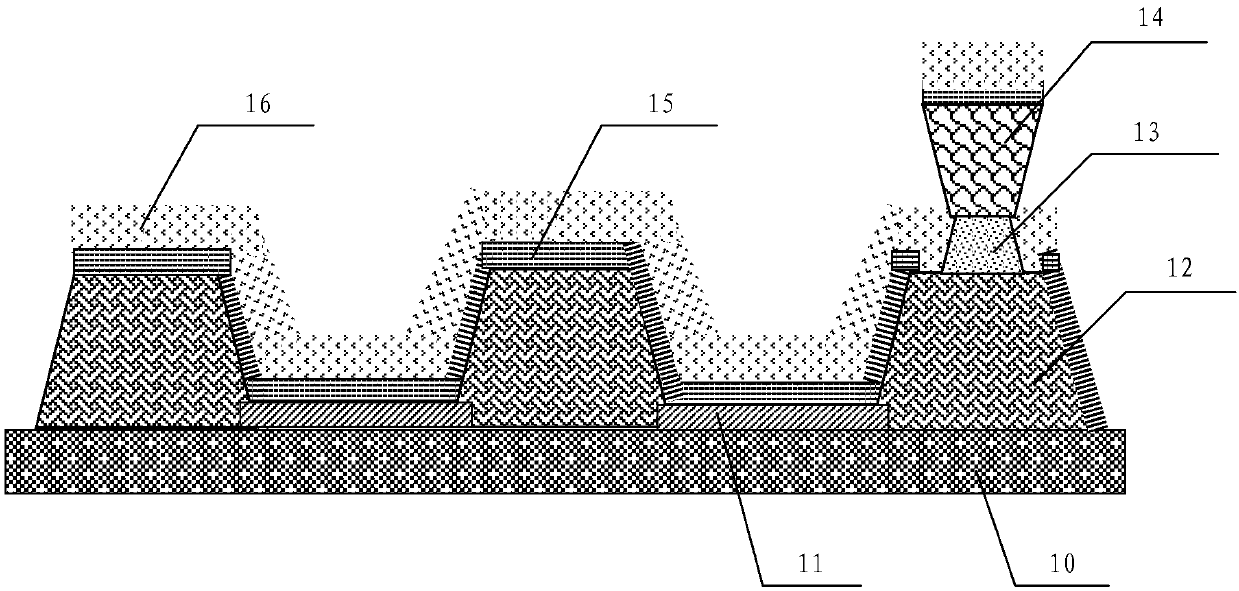
[0046] refer to figure 1 , shows a schematic cross-sectional structure of an array substrate provided in Embodiment 1 of the present application, the array substrate includes a substrate 10 and an anode layer 11 and a pixel definition layer 12 patterned and formed on the substrate 10 .

[0047] An auxiliary cathode layer 13 formed on the pixel definition layer 12 , and a spacer layer 14 formed on the auxiliary cathode layer 13 .

[0048] The organic light emitting layer 15 covering the anode layer 11 , the pixel definition layer 12 and the spacer layer 14 .

[0049] The cathode layer 16 covering the organic light emitting layer 15 .

[0050] Specifically, the substrate 10 may be a BP substrate with a thin film transistor array fabricated, and may also include a planarization layer formed on the BP substrate, wherein the material of the planarization layer may be Resin, PDL, SiNx and other materials.

[0051] The anode layer 11 formed on the substrate 10 by patterning may be ...

Embodiment 2

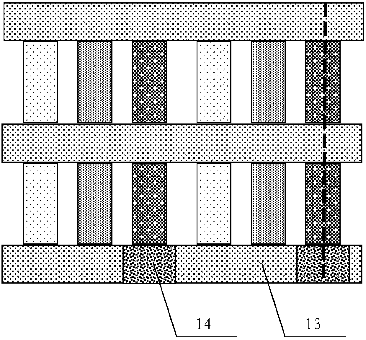
[0061] Embodiment 2 of the present application provides an array substrate, referring to figure 2 The auxiliary cathode layer 13 of the array substrate includes a plurality of auxiliary cathode strips arranged in parallel, and the spacer layer 14 includes a plurality of spacer columns arranged in an array on the auxiliary cathode layer 13. In the directions parallel to and perpendicular to the cathode strips, a spacer column is provided corresponding to every three sub-pixels.

[0062] figure 2 The schematic diagram of the cross-sectional structure corresponding to the position of the dotted line in the middle is as follows: figure 1 As shown, where the dotted line corresponds to the direction of the center line of the pixel unit adjacent to the spacer column, the cross section of the spacer column in this direction is an inverted trapezoid, and the short side of the inverted trapezoid is close to the auxiliary cathode layer 13; and In this direction, the orthographic proj...

Embodiment 3

[0067] Embodiment 3 of the present application provides a display device, including the array substrate described in any one of the above embodiments.


PUM


Abstract

The invention provides a preparation method of an array substrate, the array substrate and a display device. The array substrate comprises a substrate, anode layers, pixel definition layers, auxiliarycathode layers, spacer layers, an organic light-emitting layer and a cathode layer, wherein the anode layers and the pixel definition layers are formed on the substrate in a patterning manner; the auxiliary cathode layers and the spacer layers are arranged on the corresponding pixel definition layers in a laminating manner; the organic light-emitting layer covers the anode layers, the pixel definition layers and the spacer layers; and the cathode layer covers the organic light-emitting layer and overlaps with the auxiliary cathode layers on the pixel definition layers. The auxiliary cathode layers are arranged on the corresponding pixel electrode layers and correspond to non-display areas, so that a material with low resistivity can be selected by the auxiliary cathode layers, the resistance can also be further reduced through increasing the thickness, and an IR Drop of the cathode layer overlapping with the auxiliary cathode layers is also correspondingly reduced, thereby improving the uniformity of the characteristics, such as the display brightness of a screen and improving the display quality of the screen.

Description

technical field [0001] The invention relates to the field of photoelectric display technology, in particular to a method for preparing an array substrate, an array substrate and a display device. Background technique [0002] Organic Light Emitting Display (OLED), also known as organic electroluminescent display in Japan, is a flat-panel display device in which organic materials emit light through carrier injection and recombination driven by an electric field. Compared with the currently dominant liquid crystal display (LCD) and plasma display (PDP), OLED has low cost, all solid state, active light emission, high brightness, high contrast, wide viewing angle, fast response, thin thickness, low voltage DC Drive, low power consumption, wide operating temperature range, and soft screen display can be realized. It is an ideal flat panel display. [0003] Among them, the top-emitting OLED device can significantly increase the aperture ratio of the OLED device, and at the same t...

Claims


Application Information

Patent Timeline
Patent Type & Authority Applications(China)
IPC IPC(8): H01L51/52H01L51/56H01L27/32
CPCH10K59/122H10K59/1315H10K50/824H10K71/00
Inventor 高昕伟
Owner BOE TECH GRP CO LTD
Why Eureka
Try Eureka