Amoled display panel and preparation method thereof
A technology for display panels and substrates, applied in the fields of semiconductor/solid-state device manufacturing, semiconductor devices, electrical components, etc., can solve the problems of low yield and high cost, and achieve the effect of improving yield, reducing height, and facilitating thinning
- Summary
- Abstract
- Description
- Claims
- Application Information
AI Technical Summary
Problems solved by technology
Method used
Image
Examples
Embodiment 1
[0042] An embodiment of the present invention provides a method for preparing an AMOLED display panel, comprising the following steps:
[0043] S1, providing a substrate. Wherein, the substrate is preferably but not limited to a transparent substrate.
[0044] S2, preparing the shielding metal part and the anode on the same layer on the substrate. Wherein, the shielding metal part is used to shield the external light signal from illuminating the active layer through the substrate; the anode serves as an electrode of the OLED light-emitting device.
[0045] S3, preparing a TFT structure on a substrate with a shielding metal part and an anode, the TFT structure includes an active layer, a gate insulating layer, a gate, a source and a drain, and the drain is electrically connected to the anode. In this embodiment, the TFT structure is a top-gate structure, of course, the TFT structure in the present invention can also be a bottom-gate structure; the gate insulating layer is loc...
Embodiment 2
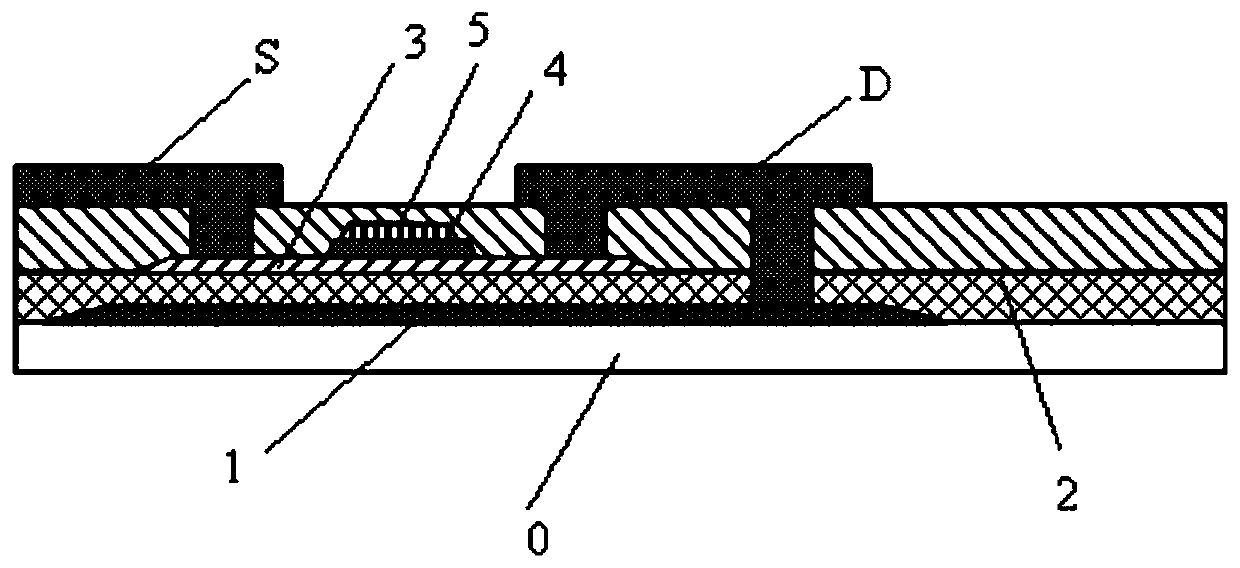
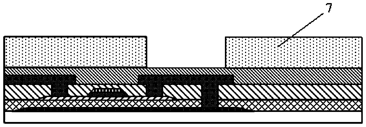
[0069] see Figure 2h , the embodiment of the present invention also provides an AMOLED display panel, including a substrate 20; on the same layer of the substrate 20, a shielding metal part 21 and an anode 22 are arranged; on the substrate 20 having the shielding metal part 21 and the anode 22, a TFT is arranged structure, the TFT structure includes an active layer 40, a gate insulating layer 50, a gate 60, a source S and a drain D; the drain D is electrically connected to the anode 22; an organic light-emitting layer 100 is arranged on a substrate 20 having a TFT structure and the cathode 110 , the organic light emitting layer 100 is located between the anode 22 and the cathode 110 and connected to the anode 22 and the cathode 110 .
[0070] In the AMOLED display panel provided by the embodiment of the present invention, since the shielding metal part 21 and the anode 22 are provided on the same layer on the substrate, the shielding metal part 21 and the anode 22 can be form...
Embodiment 3
[0081] An embodiment of the present invention further provides an AMOLED display device, including the AMOLED display panel provided in the above embodiment.
[0082] It should be noted that the display device may also include other auxiliary structures such as supports.
[0083] The AMOLED display device provided by the embodiment of the present invention adopts the AMOLED display panel provided by the above-mentioned embodiment 2, so it not only saves the process time, reduces the cost and improves the yield; but also can reduce the height of the display panel, which is beneficial to the display substrate. thinning.
PUM
 Abstract
Description
Claims
Application Information
 - R&D
- Intellectual Property
- Life Sciences
- Materials
- Tech Scout
- Unparalleled Data Quality
- Higher Quality Content
- 60% Fewer Hallucinations
Browse by: Latest US Patents, China's latest patents, Technical Efficacy Thesaurus, Application Domain, Technology Topic, Popular Technical Reports.
© 2025 PatSnap. All rights reserved.Legal|Privacy policy|Modern Slavery Act Transparency Statement|Sitemap|About US| Contact US: help@patsnap.com


