Thick copper circuit board and circuit etching and solder-resisting manufacturing methods thereof

A technology for thick copper circuit boards and circuit boards, which is used in the manufacture of printed circuits, removal of conductive materials by chemical/electrolytic methods, and printed circuits. and other problems, to achieve the effect of solving the problem of circuit etching, solving the soldering resistance of the circuit, and solving the problem of the soldering resistance of the circuit.

Inactive Publication Date: 2010-10-13
昆山华升电路板研发基地有限公司
View PDF0 Cites 38 Cited by
  • Summary
  • Abstract
  • Description
  • Claims
  • Application Information

AI Technical Summary

Problems solved by technology

However, the thick copper plate in the past can only be 0.5-6oz, and the ultra-thick copper plate has been ignored because it cannot solve the problems of line etching and solder mask production.

Method used


Image

  • Thick copper circuit board and circuit etching and solder-resisting manufacturing methods thereof
  • Thick copper circuit board and circuit etching and solder-resisting manufacturing methods thereof
  • Thick copper circuit board and circuit etching and solder-resisting manufacturing methods thereof

Examples


Embodiment

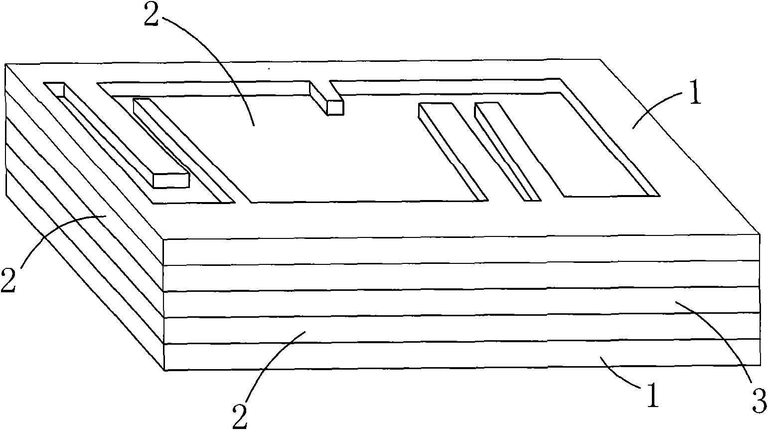
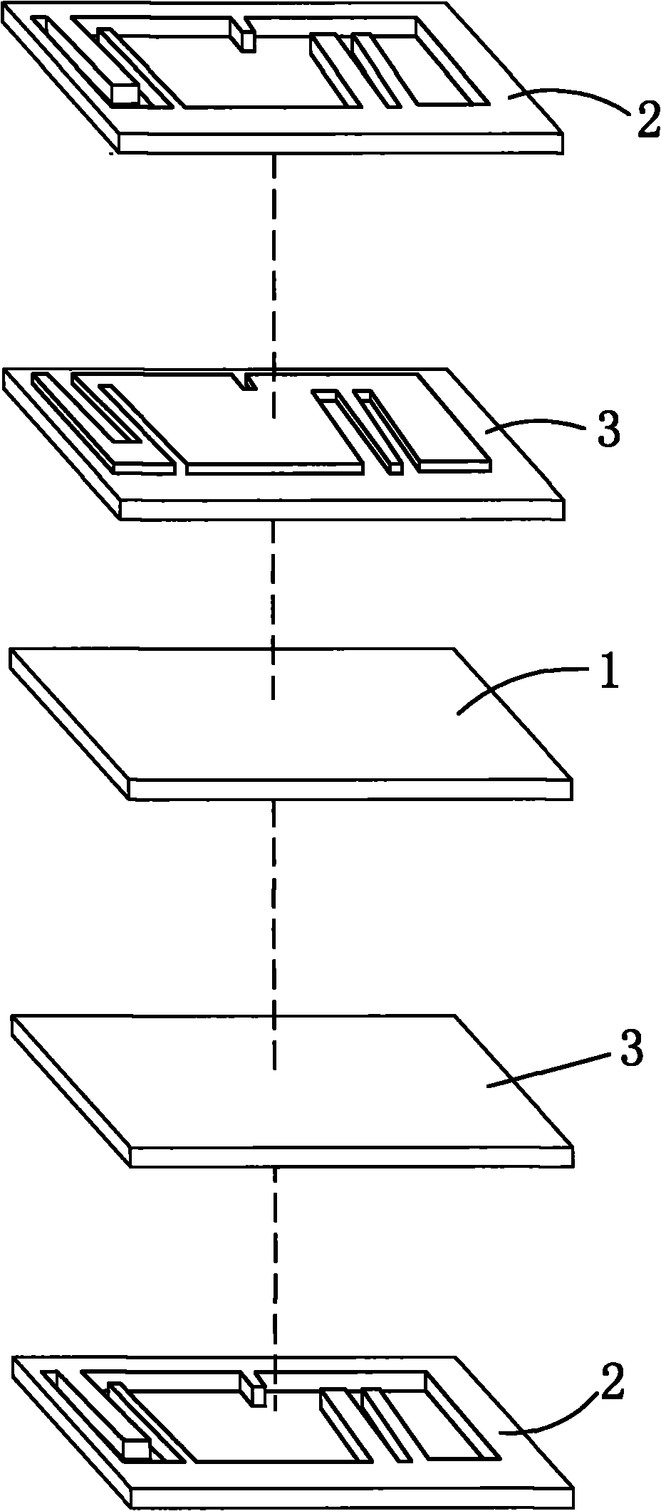
[0032] Embodiment: A thick copper circuit board, including a substrate 1, several thick copper circuit layers 2 and several thermally conductive insulating layers 3, both surfaces of the substrate 1 are covered with thermally conductive insulating layers 3, and the surface of the thermally conductive insulating layer 3 is covered with thick copper circuit layers 2, which conduct heat The insulating layer 3 and the thick copper circuit layer 2 are in the shape of intersecting interlayers covering each other, and the thick copper circuit layer 2 in contact with each thermally conductive insulating layer 3 is partially embedded in the contacting thermally conductive insulating layer 3 from the contact surface (referring to the thickness Part of the thickness of the copper circuit layer 2 is embedded in the thermally conductive insulating layer 3), and the surface of the thick copper circuit layer 2 on the surface of the circuit board is covered with a solder resist layer.

[0033]...


PUM


Abstract

The invention discloses a thick copper circuit board and circuit etching and solder-resisting manufacturing methods thereof. Thick copper circuit layers in the circuit board, which contact with heat-conducting insulation layers, are partially embedded into the contacting heat-conducting insulation layers from contact faces. In the manufacture of the structure, the thick copper circuit layers are manufactured by a mode of etching both faces of an ultra-thick copper foil respectively, and the problem of circuit etching of the ultra-thick copper foil is solved; prepregs with high resin content are adopted as the heat-conducting insulation layers, the laminated heat-conducting insulation layers are partially filled into the circuit clearances of the thick copper circuit layers, the height of the thick copper circuit layers arranged at both faces of the circuit board and exposed out of the circuit board is effectively lowered, and the problem of solder resisting of the circuit of the ultra-thick copper foil is solved; the manufacturing process is the prior art and has low cost; and the copper thickness of the circuit layers is greater than 6oz, and the invention has favorable heat conductivity, electric signal interference shielding property and superior supervoltage loading property.

Description

technical field [0001] The invention relates to the field of circuit boards, in particular to the field of thick copper circuit boards and their manufacture. Background technique [0002] With the rapid development of the electronics industry, the size of electronic products is getting smaller and smaller, and the power density is getting higher and higher. Solving the heat dissipation problem of electronic products has been raised to a new height. Ultra-thick copper plates have good thermal conductivity and electrical conductivity. Signal interference shielding and excellent ultra-high voltage load performance, its appearance is undoubtedly one of the effective means to solve this problem. However, the thick copper plate in the past can only be 0.5-6oz, and the ultra-thick copper plate has been ignored because it cannot solve the problems of line etching and solder mask production. Contents of the invention [0003] In order to overcome the above-mentioned defects, the p...

Claims


Application Information

Patent Timeline
Patent Type & Authority Applications(China)
IPC IPC(8): H05K1/02H05K3/00H05K3/06
Inventor 黄坤唐雪明曹庆荣
Owner 昆山华升电路板研发基地有限公司
Why Eureka
Try Eureka