A fan-out packaging method

A packaging method and fan-out technology, which is applied in the direction of semiconductor/solid-state device parts, semiconductor devices, electrical components, etc., can solve the problems of large node spacing of packaging substrates, chip offset, and difficulty in lithography alignment, and achieves a certain Conducive to heat dissipation, improved packaging accuracy, good thermal conductivity

Active Publication Date: 2021-09-21
NANTONG FUJITSU MICROELECTRONICS
View PDF7 Cites 0 Cited by
  • Summary
  • Abstract
  • Description
  • Claims
  • Application Information

AI Technical Summary

Problems solved by technology

[0004] The inventors of the present invention have found in the long-term research process that the above-mentioned fan-out packaging method directly connects the chip to the packaging substrate, and the node spacing of the packaging substrate is relatively large, which cannot be used for high-precision chips; secondly, in the fan-out packaging method, due to When the plastic film is used, the temperature changes during the plastic sealing of the chip will cause the film to shrink and warp due to the difference in the coefficient of thermal expansion (CTE) of the plastic sealing material, chip and carrier board during plastic sealing, which will cause the chip to shift during plastic sealing. The offset causes difficulties in subsequent processes such as lithography alignment

Method used


Image

  • A fan-out packaging method
  • A fan-out packaging method
  • A fan-out packaging method

Examples


Embodiment Construction

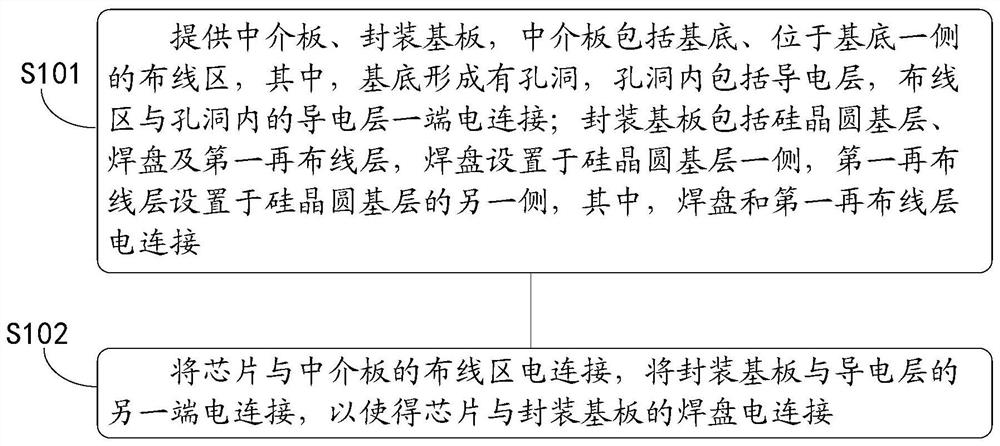
[0028] see figure 1 , figure 1 It is a schematic flow chart of an embodiment of the fan-out packaging method of the present invention, the method includes:

[0029] S101: Provide an interposer and a packaging substrate. The interposer includes a base and a wiring area on one side of the base, wherein the base is formed with a hole, the hole includes a conductive layer, and the wiring area is electrically connected to one end of the conductive layer in the hole; the packaging substrate includes The base layer of the silicon wafer, the pad and the first rewiring layer, the pad is arranged on one side of the base layer of the silicon wafer, and the first rewiring layer is arranged on the other side of the base layer of the silicon wafer, wherein the pad and the first rewiring layer layer electrical connection;

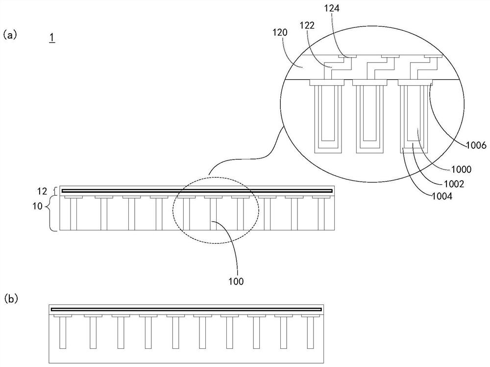
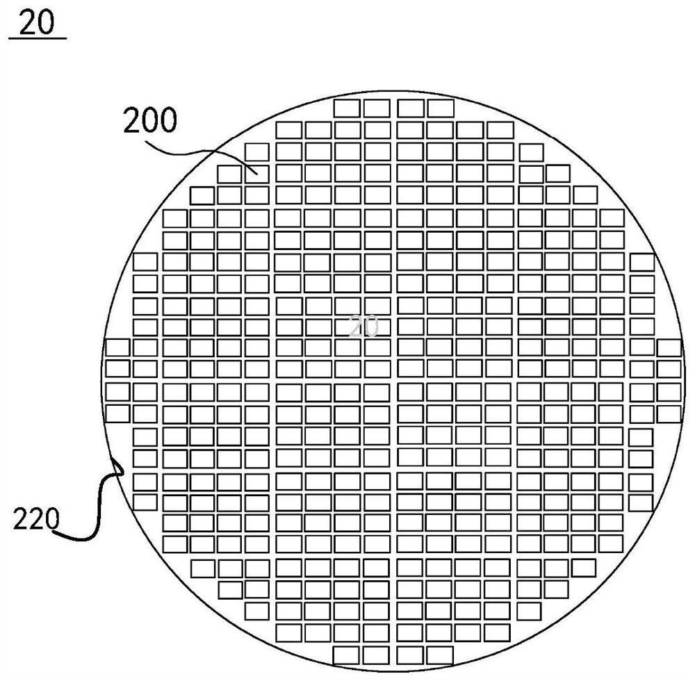
[0030] In an application scenario, such as figure 2 as shown, figure 2 for figure 1 A schematic structural diagram of an embodiment of an interposer. The interpos...


PUM


Abstract

The invention discloses a fan-out packaging method, which includes: providing an interposer and a packaging substrate, the interposer includes a base and a wiring area on one side of the base, wherein the base is formed with a hole, and the hole Including a conductive layer, the wiring area is electrically connected to one end of the conductive layer in the hole; the packaging substrate includes a silicon wafer base layer, a pad and a first rewiring layer, and the pad is arranged on the On one side of the base layer of the silicon wafer, the first rewiring layer is arranged on the other side of the base layer of the silicon wafer, wherein the pad is electrically connected to the first rewiring layer; the chip is connected to the intermediary The wiring area of ​​the board is electrically connected to electrically connect the package substrate to the other end of the conductive layer, so that the chip is electrically connected to the pad of the package substrate. Through the above method, the embodiment provided by the present invention can improve the precision of the fan-shaped packaging and prevent the chips from shifting.

Description

technical field [0001] The invention relates to the technical field of semiconductor packaging, in particular to a fan-out packaging method. Background technique [0002] With the development of semiconductor technology, the size of the chip is getting smaller and smaller, and the density of I / O (input / output) pins on the surface of the chip is getting higher and higher. High density I / O pins fan out to low density package pins. [0003] At present, the existing fan-out packaging method includes the following process: providing a carrier board, attaching a layer of double-sided adhesive film on the carrier board, attaching the front side of the chip to the adhesive film, plastic sealing the chip, and peeling off the adhesive film. Film and carrier board, forming rewiring layer, ball planting, and dicing on the front side of the chip. [0004] The inventors of the present invention have found in the long-term research process that the above-mentioned fan-out packaging metho...

Claims


Application Information

Patent Timeline
Patent Type & Authority Patents(China)
IPC IPC(8): H01L21/56H01L21/60H01L23/373
CPCH01L2224/16225H01L2924/181H01L2924/00012
Inventor 俞国庆
Owner NANTONG FUJITSU MICROELECTRONICS
Why Eureka
Try Eureka