

Routing tape machining method for circuit board
A processing method and circuit board technology, applied in printed circuit, printed circuit manufacturing, electrical components, etc., can solve the problems of size, large displacement deviation, lack of dimensional stability, product scrapping, etc., and achieve high pass rate and good product performance , The effect of easy production and operation
- Summary
- Abstract
- Description
- Claims
- Application Information
AI Technical Summary
Problems solved by technology
Method used
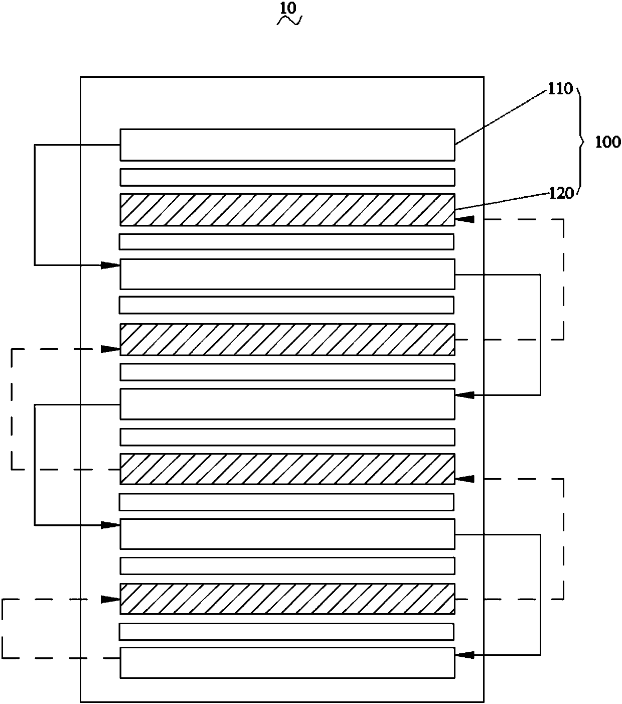
Image

Examples
Embodiment Construction
[0018] In order to facilitate the understanding of the present invention, the present invention will be described more fully below with reference to the associated drawings. Preferred embodiments of the invention are shown in the accompanying drawings. However, the present invention can be embodied in many different forms and is not limited to the embodiments described herein. On the contrary, the purpose of providing these embodiments is to make the disclosure of the present invention more thorough and comprehensive.
[0019] It should be noted that when an element is referred to as being “fixed” to another element, it can be directly on the other element or there can also be an intervening element. When an element is referred to as being "connected to" another element, it can be directly connected to the other element or intervening elements may also be present. The terms "vertical," "horizontal," "left," "right," and similar expressions are used herein for purposes of ill...
PUM
 Abstract
Description
Claims
Application Information