A composite function p-type electrode of vertical structure deep ultraviolet LED and its preparation method
A composite function, vertical structure technology, applied in circuits, electrical components, nanotechnology for materials and surface science, etc. Laser lift-off yield, good adhesion and support, the effect of reducing the threshold energy density
- Summary
- Abstract
- Description
- Claims
- Application Information
AI Technical Summary
Problems solved by technology
Method used
Image
Examples
preparation example Construction
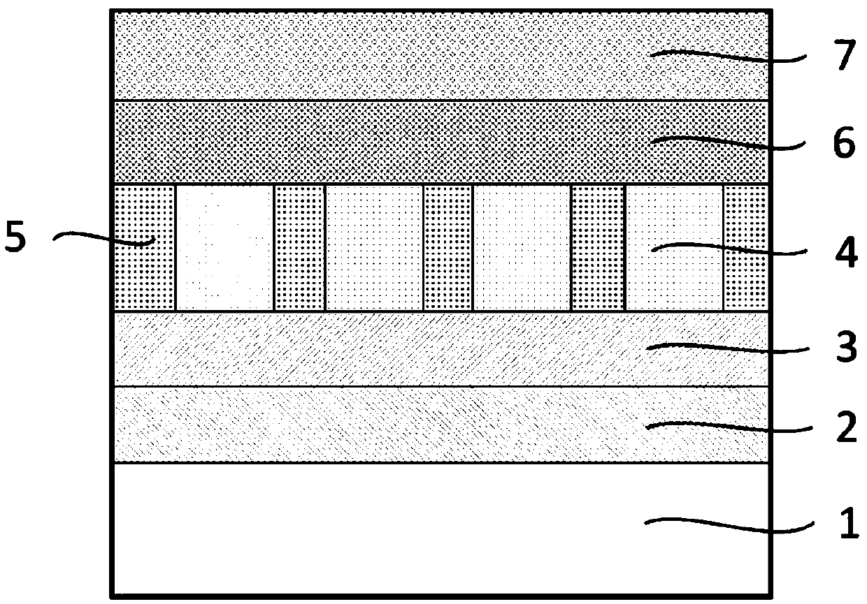
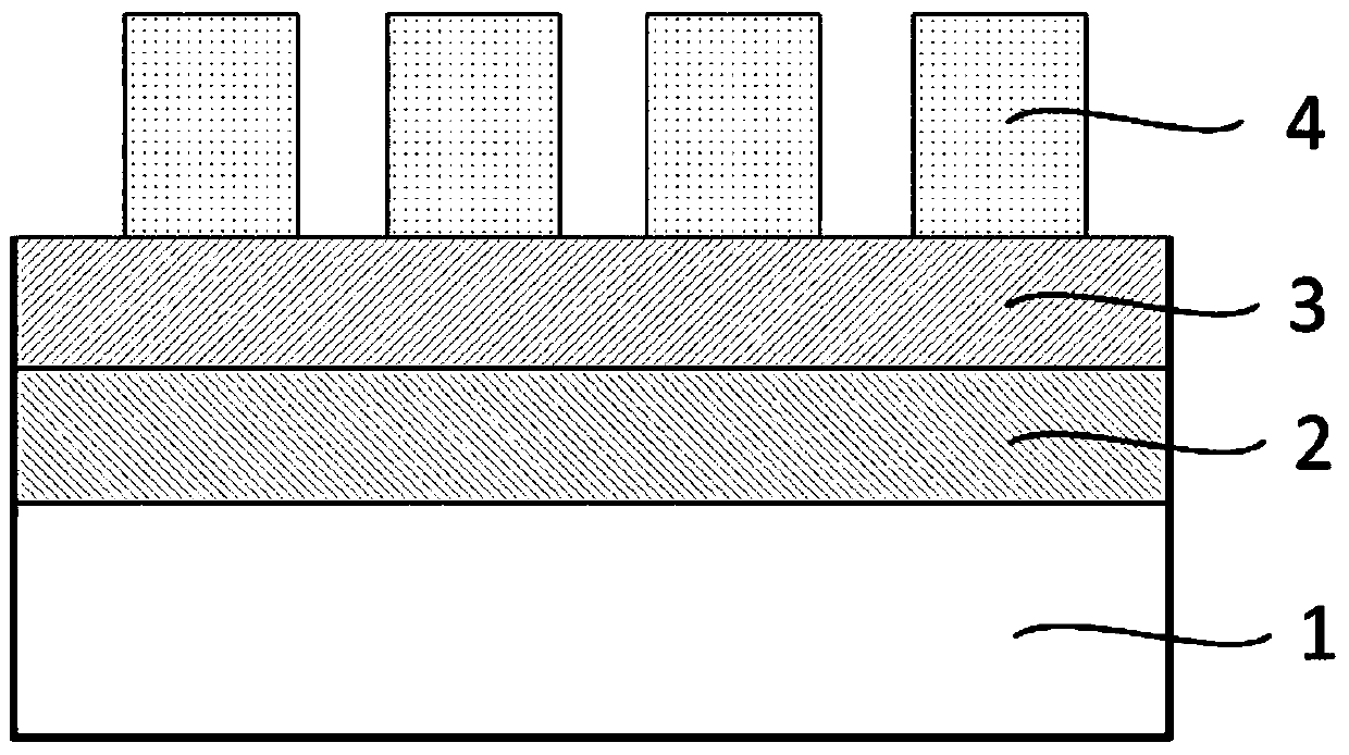
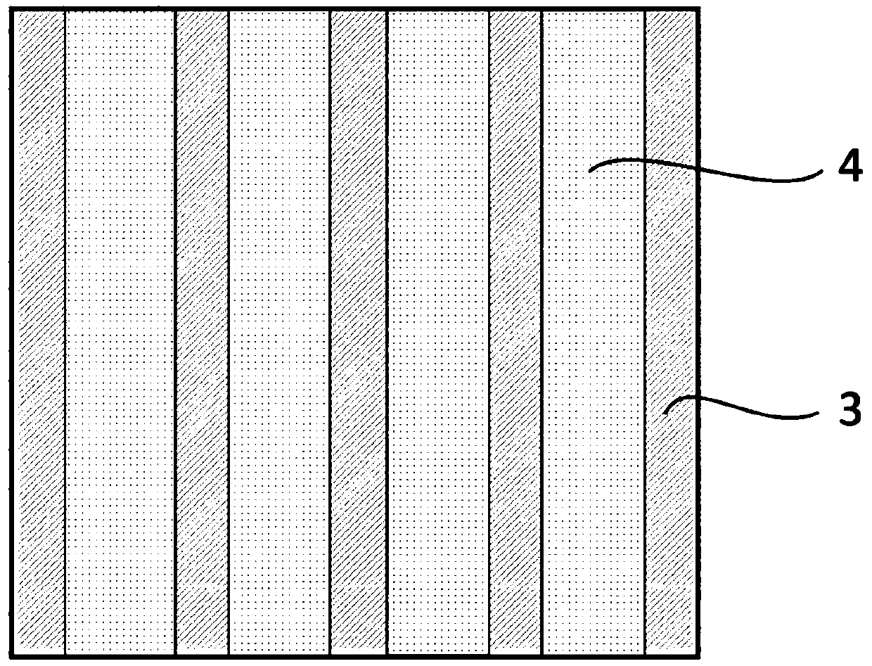
[0039] like figure 1 , Figure 2a , Figure 2b , Figure 3a , Figure 3b , Figure 4a , Figure 4b , Figure 5a , Figure 5b , Figure 6a and Figure 6b As shown, the preparation method of the composite function P-type electrode of a kind of vertical structure deep ultraviolet LED provided by the present invention comprises the following steps:
[0040] The first step is to grow an AlGaN-based deep ultraviolet LED epitaxial structure on a sapphire substrate, and perform in-situ annealing after the growth is completed to realize carrier activation;
[0041] In the second step, the grown AlGaN-based deep ultraviolet LED epitaxial wafer 1 was treated with H 2 SO 4 with H 2 o 2 The mixed solution is heated, then rinsed and dried;
[0042] In the third step, the surface of the P-type layer of the AlGaN-based deep ultraviolet LED epitaxial wafer obtained in the second step after cleaning is prepared through an electron beam evaporation platform or a magnetron sputterin...
Embodiment 1
[0049] Take a piece of AlGaN-based deep ultraviolet LED epitaxial wafer, put it in a concentration of 98% H 2 SO 4 with a mass percent concentration of 30% H 2 o 2 The mixed solution with a volume ratio of 3:1 was heated to 120°C and soaked for 20 minutes, then rinsed with deionized water for 10 minutes, and finally dried with nitrogen to complete the sample cleaning.
[0050] The cleaned epitaxial wafer was placed on the sample holder of the electron beam evaporation table, and a 5nm Ni adhesive layer and a 30nm Al mirror layer were sequentially evaporated.
[0051] The sample was taken out, and a cylindrical pattern mask with a diameter of 1 μm and a duty ratio of 1:1 was prepared by the nanosphere mask method.
[0052] Put the epitaxial wafer with the nanosphere mask into the electron beam evaporation station, and evaporate a 100nm Al three-dimensional composite functional layer.
[0053] Take out the sample, go through conventional processes such as glue removal and cl...
Embodiment 2
[0055] Take a piece of AlGaN-based deep ultraviolet LED epitaxial wafer, put it in a concentration of 98% H 2 SO 4 with a mass percent concentration of 30% H 2 o 2 The mixed solution with a volume ratio of 3:1 was heated to 120°C and soaked for 20 minutes, then rinsed with deionized water for 10 minutes, and finally dried with nitrogen to complete the sample cleaning.
[0056] The cleaned epitaxial wafer was placed on the sample holder of the electron beam evaporation table, and a 20nm Pt adhesive layer and a 10nm Ti mirror layer were evaporated sequentially.
[0057] The sample was taken out, and a quadrangular prism (cuboid) mask with a length of 400 nm, a height of 500 nm, and a duty ratio of 1:0.5 was prepared by nanoimprinting.
[0058] Put the masked sample into the magnetron sputtering station, and sputter a 500nm Al three-dimensional composite functional layer.
[0059] Take out the sample, go through conventional processes such as glue removal and cleaning, and pu...
PUM
 Abstract
Description
Claims
Application Information


