Bonding pad-based electroplating lead design

A technology of electroplating lead wires and pads, which is applied to printed circuit components, electrical connection printed components, and electrical connection formation of printed components. , to achieve the effect of reducing the impact and avoiding appearance problems

Inactive Publication Date: 2018-02-16
SHENZHEN SUNTAK MULTILAYER PCB
View PDF6 Cites 6 Cited by
  • Summary
  • Abstract
  • Description
  • Claims
  • Application Information

AI Technical Summary

Problems solved by technology

[0005] The present invention aims at the problem of signal integrity caused by residual leads after etching in the electroplating lead method of the existing circuit board and the problem of thin and broken signal lines caused by over-etching when etching the leads, and provides a pad-based electroplating lead design, The method arranges electroplating leads between the pads, which solves the signal integrity problem caused by the residue of the lead after etching in the current electroplating lead design, avoids the problem of thin and broken lines caused by the erosion of the signal lines in the current etching and plating process, and avoids the problem of Appearance problems caused by residual leads after assembly into PCBA

Method used


Image

  • Bonding pad-based electroplating lead design
  • Bonding pad-based electroplating lead design
  • Bonding pad-based electroplating lead design

Examples


Embodiment

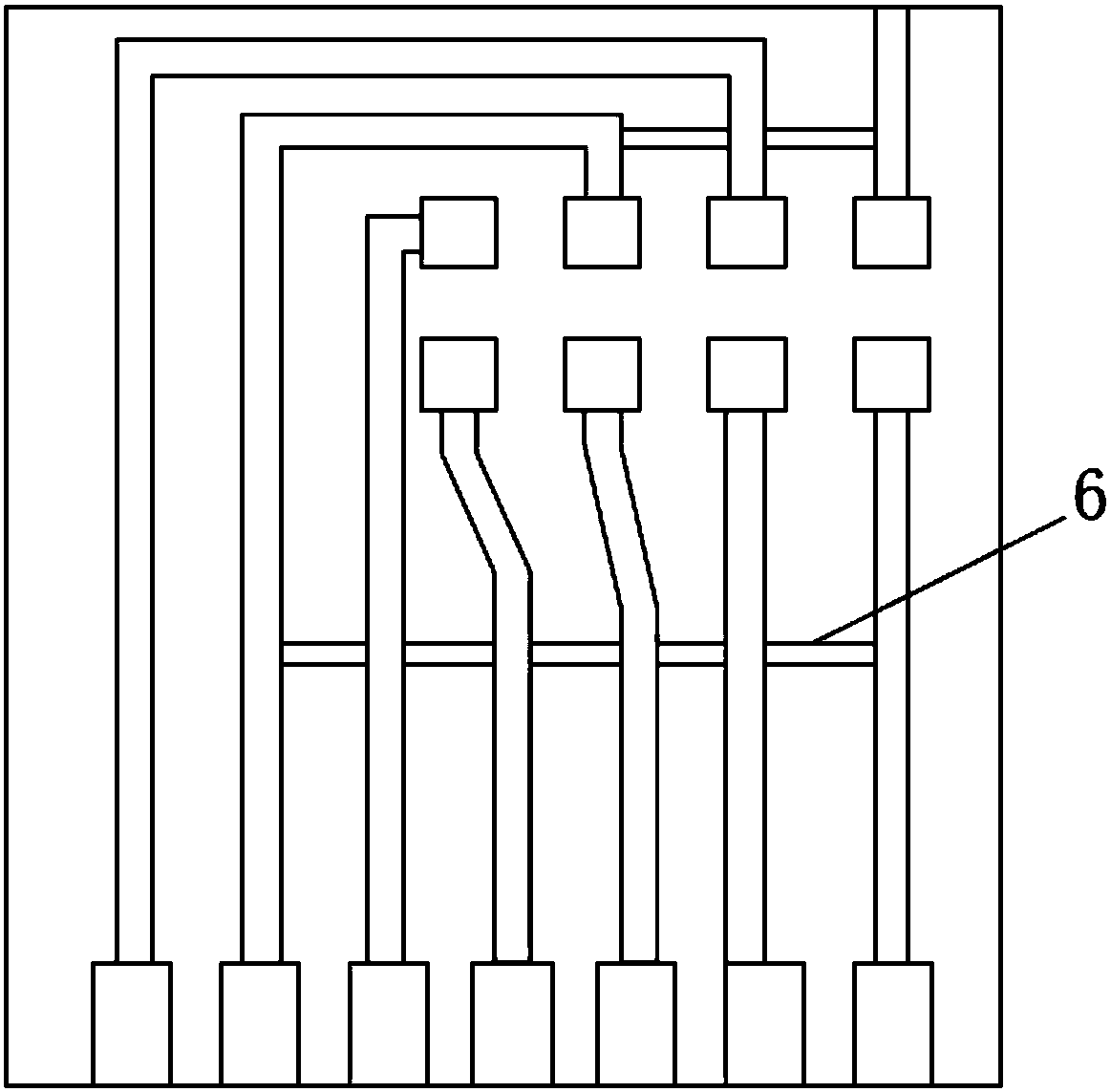
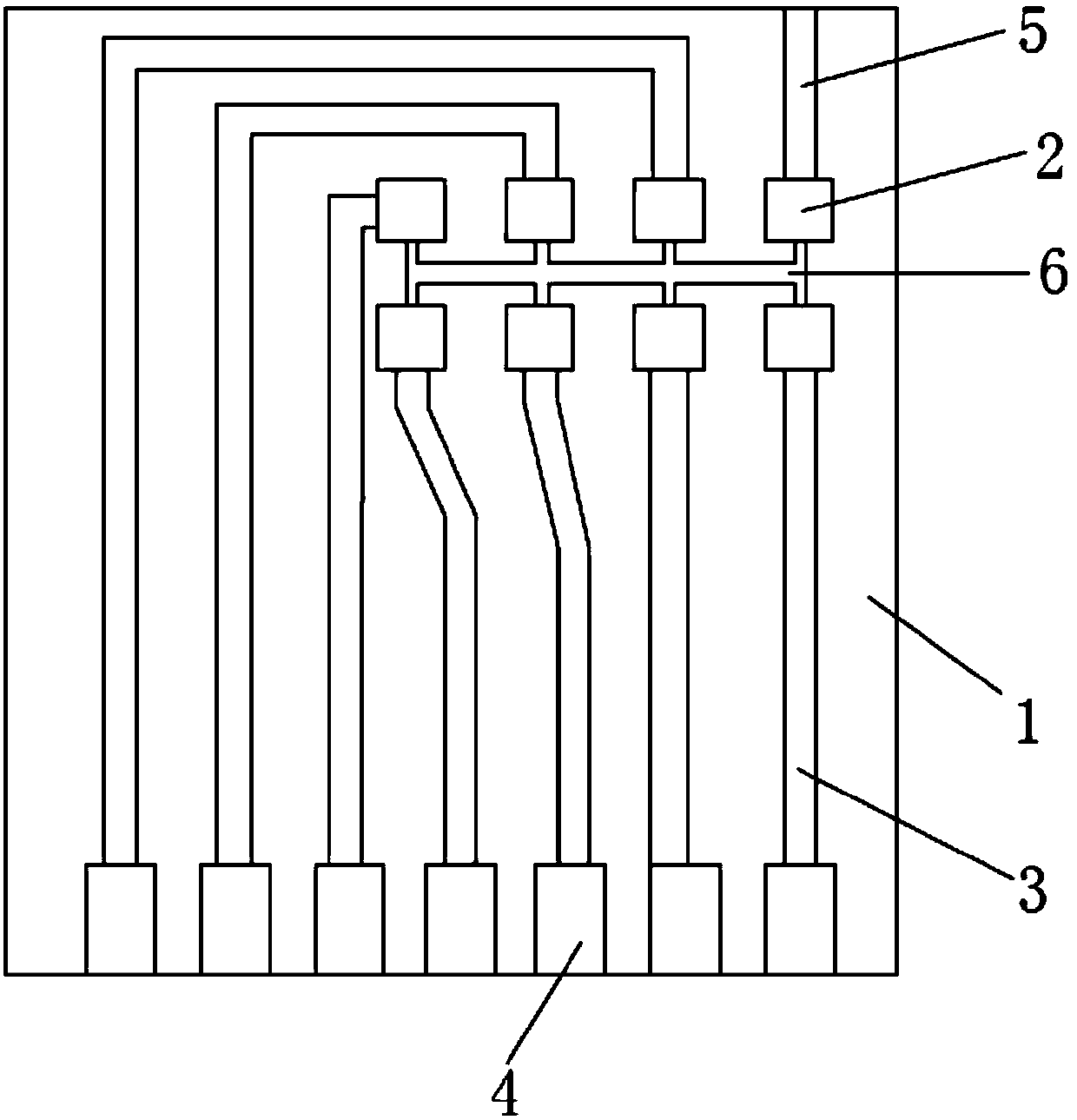
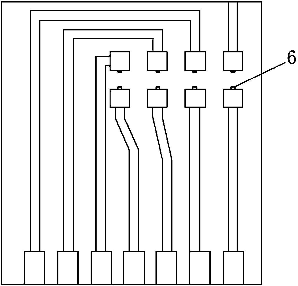
[0019] Such as figure 2 As shown, a kind of pad-based electroplating lead design shown in this embodiment includes 8 pads 2 arranged on the circuit board 1, wherein 7 pads 2 are connected to the circuit board provided on the circuit board through the signal line 3 respectively. The gold fingers 4 are connected, and the remaining 1 pad 2 is connected to the edge of the circuit board 1 through the wire 5. The 8 pads 2 are arranged in 2 rows and 4 columns, and the electroplating lead 6 is set in the middle of the 2 rows of pads 2, and the electroplating The leads 6 are connected to the eight pads 2 on both sides, so that the eight pads 2 communicate with each other through the electroplating leads 6 , and the electroplating leads 6 communicate with the electroplating current through the wires 5 connected to the edge of the board through the pads 2 .

[0020] Wherein the signal line 3 and the wire 5 and the electroplating lead 6 are separately arranged on two opposite sides of th...


PUM


Abstract

The invention discloses a bonding pad-based electroplating lead design. The bonding pad-based electroplating lead design comprises a plurality of bonding pads, wherein the plurality of bonding pads are arranged on a circuit board and are arranged adjacent to one another in a concentrated way, an electroplating lead is arranged among the plurality of bonding pads and is connected with the bonding pads at two sides, so that the bonding pads communicate with one another via the electroplating lead and finally communicate with an electroplating current. According to the method, the electroplatinglead is arranged among the bonding pads, the problem that an existing electroplating lead is additionally arranged on a signal line and the lead is resided after etching to cause signal completeness is solved, the problem of line thinness and line breakage caused by signal line etching in an existing etching electroplating process is prevented, and the appearance problem caused by resided lead after a printed circuit board assembly (PCBA) is assembled is prevented.

Description

technical field [0001] The invention relates to the technical field of printed circuit board production, in particular to a pad-based electroplating lead design. Background technique [0002] When the circuit board has surface treatment and electroplating requirements (that is, nickel-gold plating on gold fingers, nickel-gold plating on pads, etc.), and the lines in the circuit board cannot be directly connected to the edge of the peripheral conductive plate, it is necessary to add electroplating leads. All the lines on the board are connected to the side plating power supply, so that the indirect connection with the side plating power supply is realized. This is the method of adding plating leads commonly used in the PCB electroplating process; after the surface treatment electroplating process is completed, physical Or chemically disconnect the plating leads to restore the original design intention of mutual disconnection between different lines, and achieve the electrical...

Claims


Application Information

Patent Timeline
Patent Type & Authority Applications(China)
IPC IPC(8): H05K1/11H05K3/40
Inventor 叶国俊孙保玉杨润伍赖长连
Owner SHENZHEN SUNTAK MULTILAYER PCB
Why Eureka
Try Eureka