Pixel circuit, display device and dual gate driving transistor

A dual-gate drive and pixel circuit technology, which is applied in the direction of transistors, circuits, and electric solid-state devices, can solve problems such as uneven display, and achieve the effects of reduced development costs and production costs, reduced occupied area, and simple and reliable compensation methods

Active Publication Date: 2018-03-06
HEFEI XINSHENG OPTOELECTRONICS TECH CO LTD +1
View PDF5 Cites 29 Cited by
  • Summary
  • Abstract
  • Description
  • Claims
  • Application Information

AI Technical Summary

Problems solved by technology

Therefore, the first object of the present invention is to propose a pixel circuit that can not only realize threshold voltage compensation and mobility compensation for the driving transistor at the same time, but also effectively improve the problem of uneven display caused by threshold voltage drift and mobility changes. , and the compensation method is simple and reliable

Method used


Image

  • Pixel circuit, display device and dual gate driving transistor
  • Pixel circuit, display device and dual gate driving transistor
  • Pixel circuit, display device and dual gate driving transistor

Examples


Embodiment Construction

[0027] Embodiments of the present invention are described in detail below, examples of which are shown in the drawings, wherein the same or similar reference numerals designate the same or similar elements or elements having the same or similar functions throughout. The embodiments described below by referring to the figures are exemplary and are intended to explain the present invention and should not be construed as limiting the present invention.

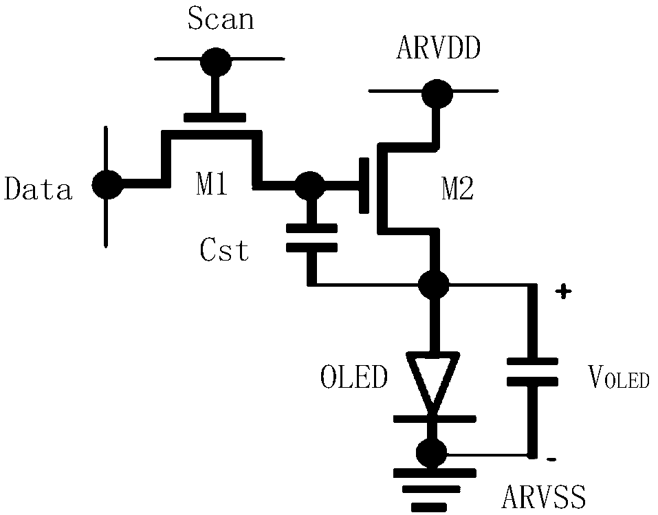
[0028] A pixel circuit, a display device, and a dual-gate driving transistor according to an embodiment of the present invention will be described below with reference to the accompanying drawings. Before describing the pixel circuit of the embodiment of the present invention, it will be explained in detail why the traditional 2T1C pixel circuit will cause uneven display due to threshold voltage shift and mobility change.

[0029] Specifically, such as figure 1As shown, the traditional 2T1C pixel circuit includes a switching tra...


PUM


Abstract

The invention discloses a pixel circuit, a display device and a dual gate driving transistor. The pixel circuit comprises a threshold voltage compensation unit, a mobility compensation unit and a light emitting control unit. The threshold voltage compensation unit is electrically connected to a data terminal and a first control terminal of an external control unit and a first gate and a source ofthe dual gate driving transistor respectively. The mobility compensation unit is electrically connected to a detection signal terminal and a second control terminal of the external control unit and the source of the dual gate driving transistor respectively. The light emitting control unit is electrically connected to the data terminal and a third control terminal of the external control unit, a second gate and the source of the dual gate driving transistor, and a light emitting device respectively. The external control unit controls the threshold voltage compensation unit and the mobility compensation unit to perform threshold voltage compensation on the dual gate driving transistor, and controls the mobility compensation unit and the light emitting control unit to perform mobility compensation on the dual gate drive transistor and control light emission of the light emitting device. As a result, the threshold voltage compensation and mobility compensation for the driving transistor at the same time can be achieved.

Description

technical field [0001] The invention relates to the field of display technology, in particular to a pixel circuit, a display device and a double-gate drive transistor. Background technique [0002] Currently, with the vigorous development of display panels, OLED (Organic Light Emitting Diode, Organic Light Emitting Diode) becomes the trend of the panel industry in the future due to its high contrast ratio and low power consumption. [0003] The traditional OLED pixel circuit is a 2T1C driving structure, specifically as figure 1 shown, but due to the instability of the driving transistor, the threshold voltage and mobility of the driving transistor need to be compensated. Usually, the way to compensate the threshold voltage includes internal compensation and external compensation, but whether it is internal compensation or external compensation, it is very difficult to realize the threshold voltage compensation and mobility compensation of the driving transistor at the same ...

Claims


Application Information

Patent Timeline
Patent Type & Authority Applications(China)
IPC IPC(8): G09G3/3208H01L51/05H01L51/10
CPCG09G3/3208H10K10/482G09G3/3233G09G2300/0819G09G2300/0852G09G2310/0262G09G2310/08G09G2320/0295G09G2320/0233G09G2320/045H10K59/125G09G3/3225H10K10/82
Inventor 冯雪欢袁志东蔡振飞李蒙袁粲
Owner HEFEI XINSHENG OPTOELECTRONICS TECH CO LTD
Why Eureka
Try Eureka