Supercharge Your Innovation With Domain-Expert AI Agents!

Scanning coil, scanning electron microscope and encapsulation device of scanning coil

A scanning coil and potting technology, which is applied in the direction of circuits, discharge tubes, electrical components, etc., can solve the problems of low working stability, poor rotational symmetry, and low imaging quality of scanning coils, and achieve high working stability, convenient processing, and High image quality effect

Active Publication Date: 2018-03-06
KYKY TECH
View PDF6 Cites 1 Cited by
  • Summary
  • Abstract
  • Description
  • Claims
  • Application Information

AI Technical Summary

Problems solved by technology

[0005] Therefore, the technical problem to be solved by the present invention is to overcome the defect that the scanning coil assembly in the prior art has poor rotational symmetry relative to the central axis, thereby providing a scanning coil with high rotational symmetry relative to the central axis
[0006] Another technical problem to be solved by the present invention is to overcome the defect that the scanning electron microscope in the prior art has low imaging quality due to the low working stability of the scanning coil, thereby providing a scanning electron microscope with high imaging quality

Method used


Image

  • Scanning coil, scanning electron microscope and encapsulation device of scanning coil
  • Scanning coil, scanning electron microscope and encapsulation device of scanning coil
  • Scanning coil, scanning electron microscope and encapsulation device of scanning coil

Examples


Embodiment 1

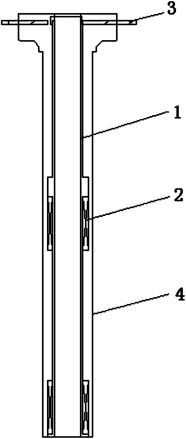
[0062] like figure 1 A specific implementation of the scanning coil of the present invention shown includes a skeleton 1, a circuit board 3 arranged on the skeleton 1, a coil 2 fixed on the skeleton 1, and the skeleton 1, The coil 2 and the circuit board 3 are packaged together with an encapsulating gel layer 4 , and the terminals of the circuit board 3 protrude from the encapsulating gel layer 4 , and the encapsulating gel layer 4 is arranged coaxially with the skeleton 1 .

[0063] The encapsulating colloid layer 4 encapsulates the framework 1, the coil 2, and the circuit board 3 into one body. The scanning coil is an integrated structure, which is convenient to install and fix in the lens barrel, and has high rotational symmetry relative to the central axis.

Embodiment 2

[0065] A scanning electron microscope of the present invention has the scanning coils provided by the above embodiments. Since the scanning coils are firmly fixed in the lens barrel, the installation centering of the scanning coils and the working stability are high, the imaging quality of the scanning electron microscope is high.

Embodiment 3

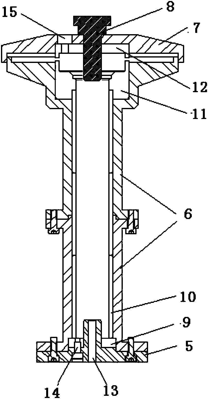
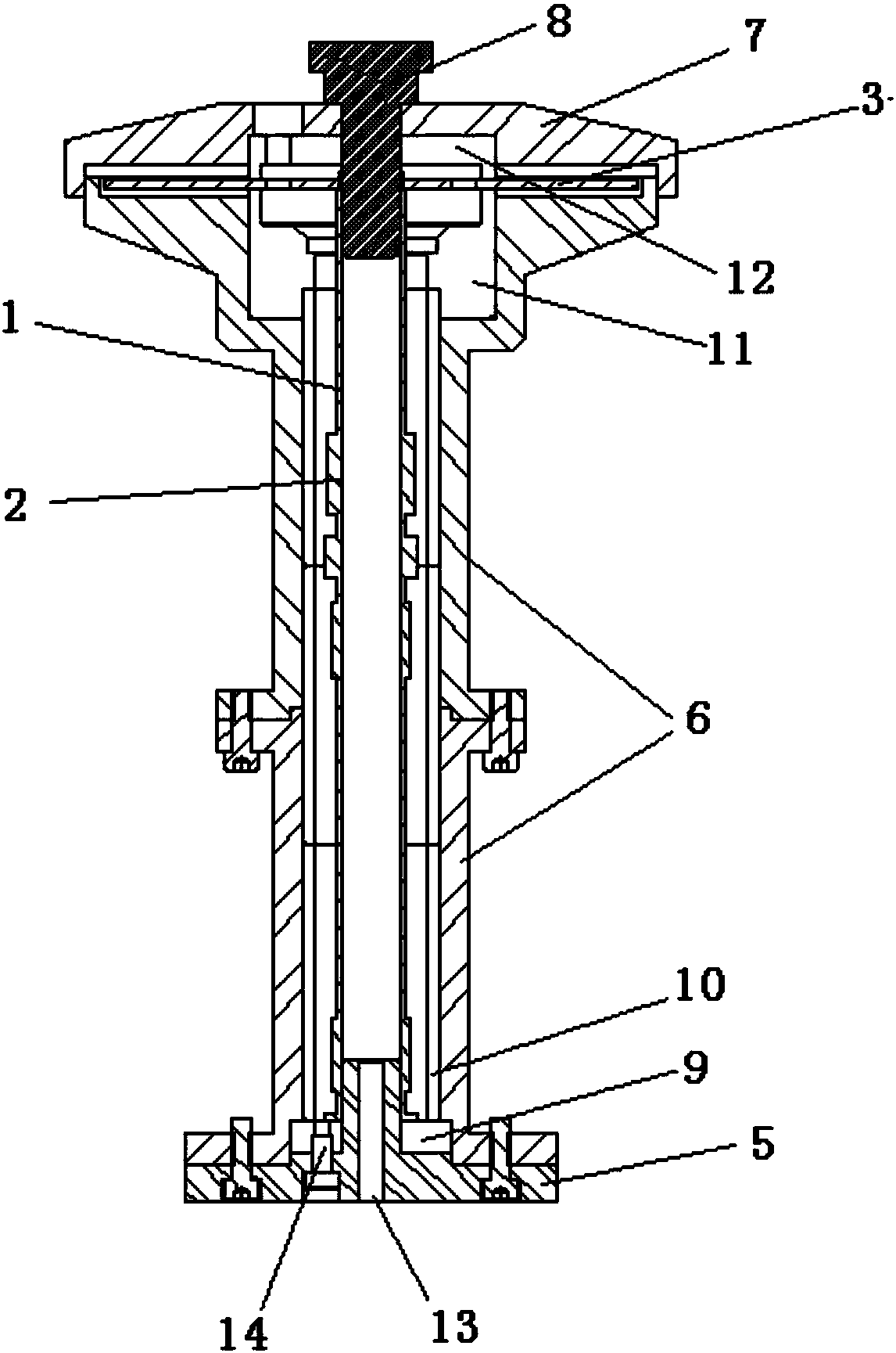
[0067] like Figure 2-3 A specific implementation of the potting device for the scanning coil shown includes a base 5; a tooling base is arranged on the base 5, and a through cavity is formed thereon; a top cover 7 is arranged on the tooling base, The top cover 7, the tooling base, and the base 5 are connected together to form a potting cavity for encapsulating the scanning coil, the terminal of the circuit board 3 is outside the potting cavity, and the base 5. At least one of the top covers 7 is provided in the potting cavity, and the scanning coil is coaxially positioned so that the axis of the skeleton 1 of the scanning coil is aligned with the axis of the potting cavity. Coaxial positioning structure; the potting port 15 is formed on the top cover 7, and the potting glue enters the potting cavity through the potting port 15 to pot the scanning coil in the potting cavity . Since at least one of the base 5 and the top cover 7 is provided in the potting cavity, the scanning...


PUM


Abstract

The invention relate to a scanning coil, a scanning electron microscope and an encapsulation device of the scanning coil. The scanning coil comprises a framework, a circuit board and a coil and also comprises a package adhesive layer, wherein the circuit board is arranged on the framework, the coil is fixed on the framework, the package adhesive layer is used for integrally packaging the framework, the coil and the circuit board, and a wiring end of the circuit board extends out of the package adhesive layer. The package adhesive layer is used for integrally packaging the framework, the coil and the circuit board, and the scanning coil is of an integrated structure, is convenient to fix in a lens cylinder and has relatively high symmetry relative to a central axis. The encapsulation deviceis provided with a positioning structure which is used for coaxially positioning the scanning coil and enabling an axis of the framework of the scanning coil and an axis of an encapsulation cavity tobe coaxial, and the scanning coil after being encapsulated can be enabled to have relatively high rotation symmetry relative to the central axis.

Description

technical field [0001] The invention relates to the technical field of scanning coil potting, in particular to a scanning coil, a scanning electron microscope and a potting device for the scanning coil. Background technique [0002] The scanning electron microscope is an electron optical instrument that scans the surface of the sample line by line with a focused electron beam. The electron beam bombards the surface of the sample to generate secondary electrons or backscattered electrons. The secondary electrons or backscattered electrons generated on the surface are collected, and the scanning position of the electron beam on the surface of the sample and the number of secondary electrons or backscattered electrons generated are represented in the form of a two-dimensional image, that is, the secondary electrons of the scanning electron microscope are obtained. image or backscattered electron image. The resolution of scanning electron microscope images can reach the nanomet...

Claims


Application Information

Patent Timeline
Patent Type & Authority Applications(China)
IPC IPC(8): H01J37/147H01J37/26H01J37/28
CPCH01J37/1474H01J37/261H01J37/28
Inventor 孟祥良
Owner KYKY TECH
Features
  • R&D
  • Intellectual Property
  • Life Sciences
  • Materials
  • Tech Scout
  • Unparalleled Data Quality
  • Higher Quality Content
  • 60% Fewer Hallucinations
Learn More