Display screen structure

A display screen and display substrate technology, which is applied in the direction of semiconductor devices, electrical components, circuits, etc., can solve the problems of small space, poor brightness of the display screen, and high brightness of the display screen

Inactive Publication Date: 2018-03-13
KUNSHAN GO VISIONOX OPTO ELECTRONICS CO LTD
View PDF3 Cites 6 Cited by
  • Summary
  • Abstract
  • Description
  • Claims
  • Application Information

AI Technical Summary

Problems solved by technology

In the current AMOLED circuit layout, due to the continuous increase of the display area of ​​the display screen, the space of the non-display area is continuously squeezed and reduced, resulting in a narrow space for the passage of lines in the non-display area. , the space that can be left for the line is usually not large, which will cause the resistance of the line to be too large, resulting in high brightness of the display screen on the side close to the power supply end, and poor brightness of the display screen on the other side away from the power supply end, resulting in The brightness of the overall display screen is inconsistent

Method used


Image

  • Display screen structure
  • Display screen structure
  • Display screen structure

Examples


Embodiment Construction

[0020] A number of embodiments of the present invention will be disclosed in the following figures. For the sake of clarity, many practical details will be described together in the following description. It should be understood, however, that these practical details should not be used to limit the invention. That is, in some embodiments of the invention, these practical details are not necessary. In addition, for the sake of simplifying the drawings, some well-known structures and components are shown in a simple schematic manner in the drawings.

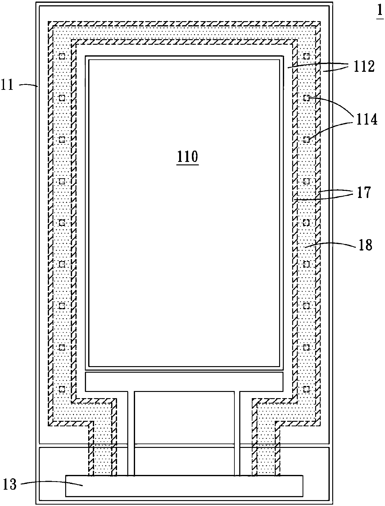
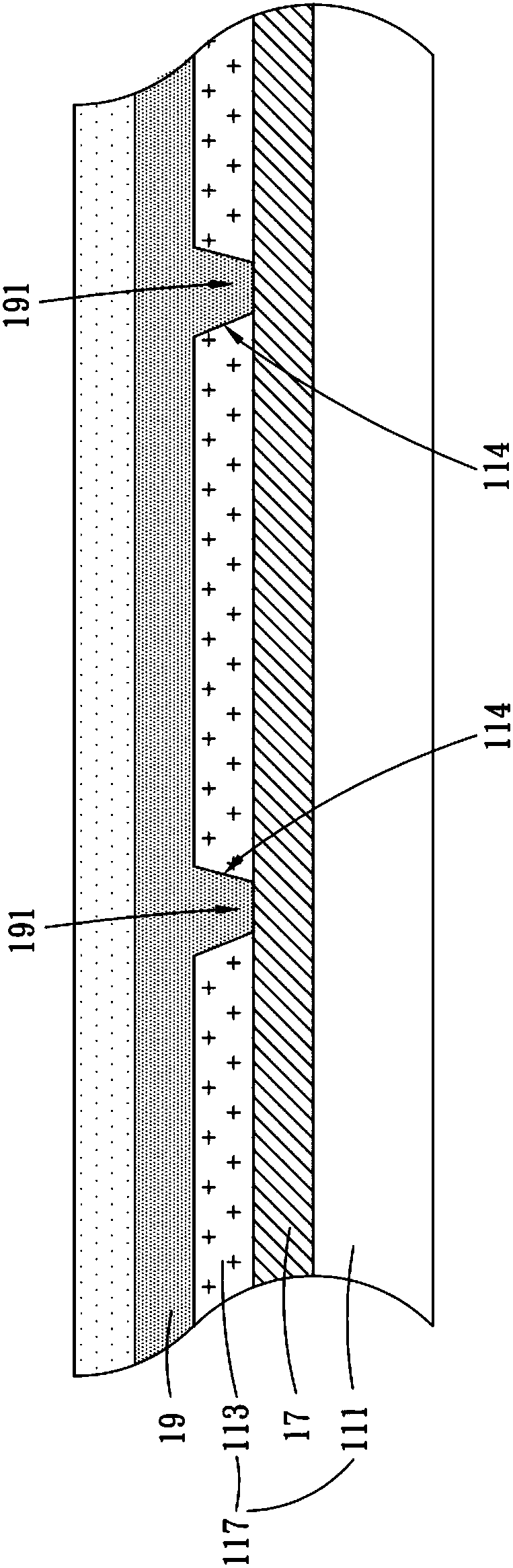
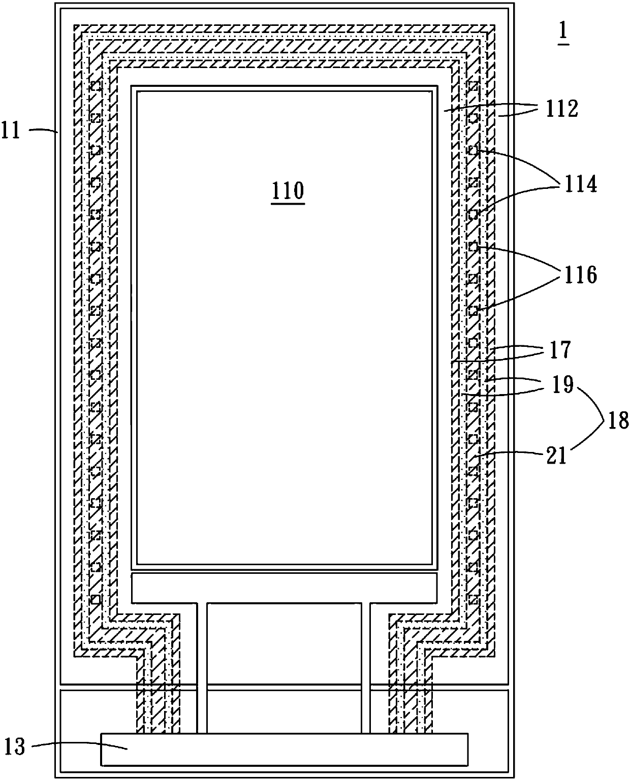
[0021] see figure 1 and figure 2 , which is a schematic diagram and a cross-sectional view of the structure of the display screen according to the first embodiment of the present invention. As shown in the figure, this embodiment provides a display screen structure 1, which is connected to each other through a plurality of metal circuit layers inside the display substrate. The voltage drop (IR drop) will not be too large, so t...


PUM


Abstract

The invention discloses a display screen structure. The display screen structure comprises a display substrate, a negative electrode wire and at least one metal circuit, wherein the display substrateis provided with a display region and a non-display region, the negative electrode wire is arranged on the non-display region, the at least one metal circuit is arranged on the non-display region andis electrically connected in parallel with the negative electrode wire, and an insulation layer is contained between the negative electrode wire and the at least one metal circuit. By such a parallelmode, the resistance in the negative electrode wire is reduced, and the brightness uniformity of a display screen is improved.

Description

technical field [0001] The invention relates to a display screen structure. Background technique [0002] With the rapid development of the electronic industry, the penetration rate of electronic products is getting higher and higher, such as computers, tablets or mobile phones and so on. The above-mentioned electronic products have become the necessities of people's daily life. Active Matrix Organic Light Emitting Diode (AMOLED) has the advantages of high chromaticity, high contrast, wide viewing angle, self-illumination and flexible display, and has been widely used. In the current AMOLED circuit layout, due to the continuous increase of the display area of ​​the display screen, the space of the non-display area is continuously squeezed and reduced, resulting in a narrow space for the passage of lines in the non-display area. , the space that can be left for the line is usually not large, which will cause the resistance of the line to be too large, resulting in high brig...

Claims


Application Information

Patent Timeline
Patent Type & Authority Applications(China)
IPC IPC(8): H01L27/32
CPCH10K59/1315
Inventor 刘权张露胡思明韩珍珍
Owner KUNSHAN GO VISIONOX OPTO ELECTRONICS CO LTD
Why Eureka
Try Eureka