Electroluminescent display panel and display device

An electroluminescence display and panel technology, applied in the direction of circuits, electrical components, electrical solid devices, etc.

Active Publication Date: 2018-03-20
WUHAN TIANMA MICRO ELECTRONICS CO LTD
View PDF6 Cites 64 Cited by
  • Summary
  • Abstract
  • Description
  • Claims
  • Application Information

AI Technical Summary

Problems solved by technology

[0003] Embodiments of the present invention provide an electroluminescent display panel and a display device, which are used to solve the problem in the prior art of how

Method used


Image

  • Electroluminescent display panel and display device
  • Electroluminescent display panel and display device
  • Electroluminescent display panel and display device

Examples


Embodiment Construction

[0016] The specific implementation manners of an electroluminescent display panel and a display device provided by the embodiments of the present invention will be described in detail below with reference to the accompanying drawings. It should be noted that the described embodiments are only some of the embodiments of the present invention, but not all of the embodiments. Based on the embodiments of the present invention, all other embodiments obtained by persons of ordinary skill in the art without making creative efforts belong to the protection scope of the present invention.

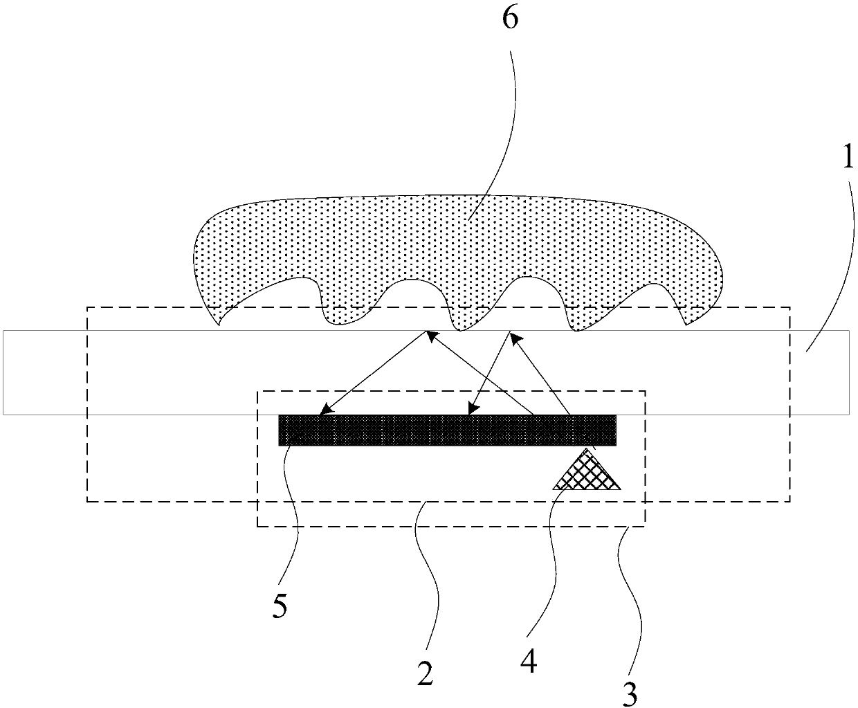
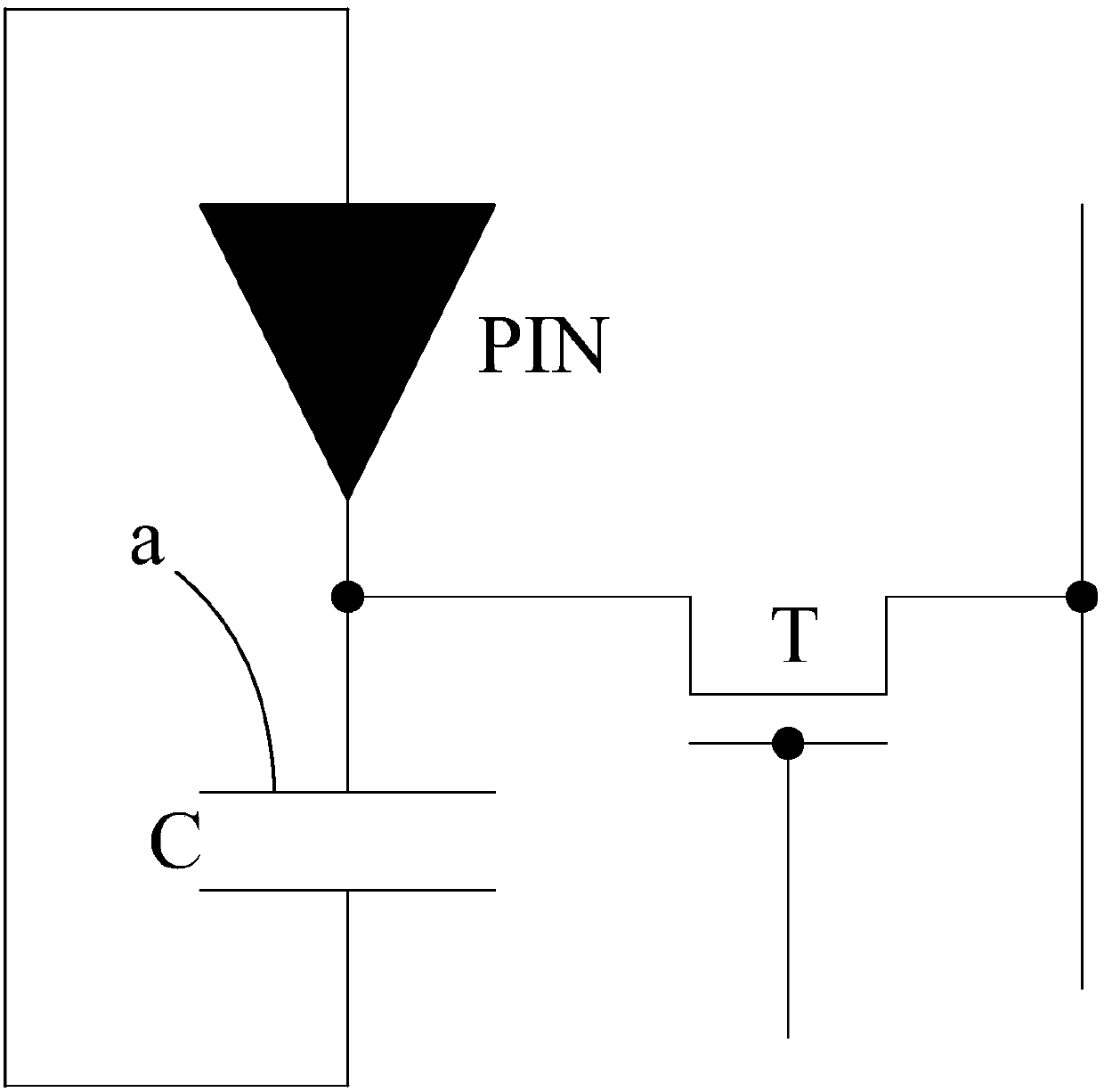
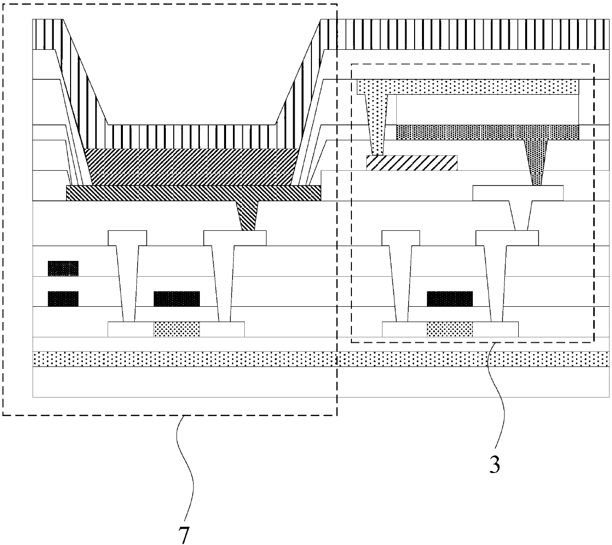
[0017] The inventor found in the research that, in figure 1 In the shown structure, only one fingerprint recognition structure is shown, and the fingerprint recognition structure 3 may include: a thin film transistor, a capacitor, a heterojunction structure and a light source 4, wherein 5 represents a fingerprint recognition structure with a thin film transistor, a capacitor and a heterojunction str...


PUM


Abstract

The invention discloses an electroluminescent display panel and a display device. According to the electroluminescent display panel and the display device, a light-sensing fingerprint identification area is arranged, so that a second light-emitting unit in a light-sensing identification pixel unit is enabled to be a transparent light emitting unit. Furthermore, during the optical fingerprint identification process, the fingerprint identification area can be used for effectively detecting fingerprints. Moreover, the light-sensing fingerprint identification area comprises a display sub-pixel unit and a light-sensing identification pixel unit. Therefore, the display function of the light-sensing fingerprint identification area can also be achieved. As a result, the occupied area of the non-display area is effectively reduced. The design of a narrow frame is facilitated.

Description

technical field [0001] The invention relates to the field of display technology, in particular to an electroluminescent display panel and a display device. Background technique [0002] Organic Light Emitting Diode (OLED) display is a self-luminous display, and has the characteristics of thinness, high chromaticity, wide viewing angle and fast response speed, and has great development prospects in the field of display technology. In order to make the display have fingerprint recognition function, such as figure 1 As shown, generally, a fingerprint identification area is provided in the non-display area 2 of the display panel 1, and a fingerprint identification structure 3 is usually provided in the fingerprint identification area; however, in figure 1 In the shown structure, since the fingerprint identification structure 3 is arranged on the non-facing side of the display panel 1, the thickness of the display panel 1 is significantly increased, which is not conducive to the...

Claims


Application Information

Patent Timeline
IPC IPC(8): H01L27/32
CPCH10K59/60H10K59/12H10K59/65H10K59/121
Inventor 马扬昭
Owner WUHAN TIANMA MICRO ELECTRONICS CO LTD
Why Eureka
Try Eureka